

Sony CXB1561Q-Y Datasheet

CXB1561Q-Y
s3R-IC for Optical Fiber Cimmunication Receiver
Description
The CXB1561Q-Y achieves the 3R optical-fiber
cimmunication receiver functions (Reshaping,
Regenerating and Retiming) on a single chip using
with a SAW filter.
Features
• 3R-IC with a built-in post-amplifier
(SAW filter system)
• Signal interruption alarm output
• Data shutdown function for signal interruption
• Timing phase can be fine adjusted
• Delay length for edge detector (differentiator) can
be selected
• Single 5V power supply
Absolute Maximum Ratings
• Supply voltage VCC – VEE –0.3 to +7.0 V
• Operating case temperature
TC –55 to +125 °C
• Storage temperatureTstg –65 to +150 °C
• Output current (surge current)
Io 0 to 50 (100) mA
• D/D input current IID –200 to +400 µA
• SC/SC input current IIC –100 to +400 µA
• S1/S2 input voltage VIS VCC to VEE + 1.2 V
Structure
Bipolar silicon monolithic IC
Applications
• SONET: 622.08Mbps, 155.52Mbps
• Fiber channel: 531.25Mbps, 265.625Mbp
• Clock multiplication: X2, X4
32 pin QFP (Ceramic)
Recommended Operating Conditions
• Supply voltage VCC – VEE 5.0 ± 0.5 V
• Operating case temperature
TC –40 to +85 °C
Sony reserves the right to change products and specifications without prior notice. This information does not convey any license by
any implication or otherwise under any patents or other right. Application circuits shown, if any, are typical examples illustrating the
operation of the devices. Sony cannot assume responsibility for any problems arising out of the use of these circuits.
– 1 –
E93615B6Z
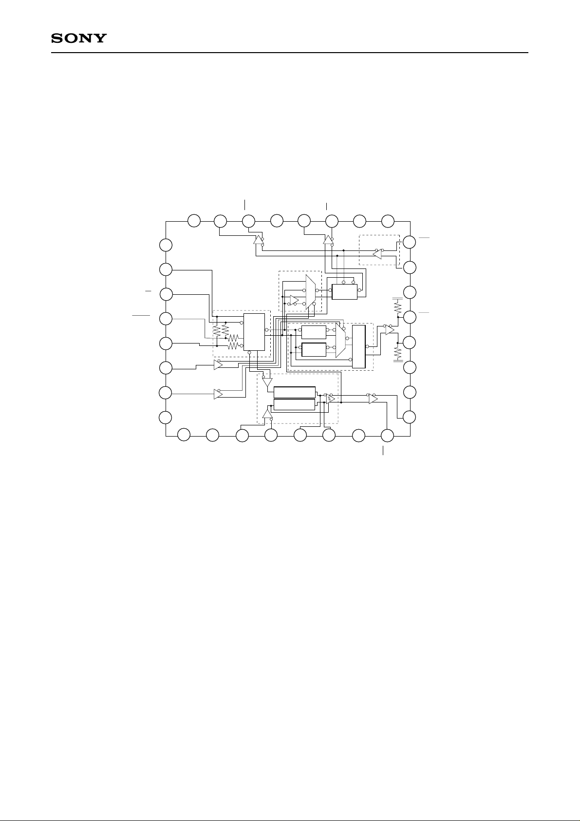
Block Diagram
24
DA
EE
V
23
CA
22
CA
21
DA
CC
V
20
CXB1561Q-Y
AL
DI
CC
CC
V
V
Q
Q
19
18
17
VEEA
CAP1
CAP1
S1
S2
VCCA
D-FF
Limit Amp
VEEDB
Differential
V
EEDB
25
26
D
27
D
28
Post
Amp
29
Delay
delay2
delay1
30
16
15
14
13
12
11
SC
SC
VEEAL
SQ
SQ
VCCDB
ALARM
31
peak hold
10
VEEDB
peak hold
SD
32
1
VccD
5
CAP2
6
CAP3
7
EE
V
2
3
D
EE
V
4
UP
DOWN
9
8
SD
– 2 –
Pin Description
CXB1561Q-Y
Pin
No.
Symbol
Typical pin voltage
DC AC
1 VccD 0V
2VEED –5V
3 UP –1.3V
4 DOWN –1.3V
5 CAP2 –1.8V
6 CAP3 –1.8V
Equivalent circuit Description
Positive power supply
pin for digital block.
Negative power supply
pin for digital block.
VCCA
1k
Resistor connection pins
for alarm level setting.
UP pin: When the
100
3
4
100
200
200
resistance connection to
this pin is increased, the
alarm level becomes
higher.
DOWN pin: When the
resistance connected to
this pin is increased, the
VEEA
0.8mA 0.8mA
alarm level becomes
lower.
Capacitance connection
pins for alarm block peak
VCCA
hold circuit.
(Each pin incorporates a
capacitance of
approximately 10pF.)
CAP2 pin: Peak hold
80
10p
5
6
80
10p
capacitance connection
pin for the post-amplifier
signal output.
5µA
5µA
CAP3 pin: Peak hold
capacitance connection
V
20µA
EEA
pin for the alarm level
setting block.
7VEE –5V Negative power supply pin.
V
CCD
8SD
–0.9V
to
–1.7V
Alarm output pins.
Terminate these pins in
9SD
10 VEEDB –5V
11 VCCDB 0V
–0.9V
to
–1.7V
8
9
VEED
510Ω at VEE.
Negative power supply
pin for differential circuit.
Positive power supply pin
for differential circuit.
– 3 –
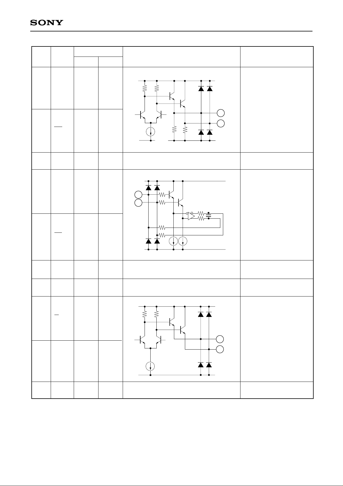
CXB1561Q-Y
Pin
Symbol Equivalent circuit Description
No.
12 SQ
Typical pin voltage
DC AC
–0.9V
to
VCCDB
–1.7V
Differential output pins.
Negative power supply
pin for limiter amplifier.
13 SQ
14 VEEAL
–5V
–0.9V
to
–1.7V
VEED
510
13
12
510
VEEDB
VCCAL
–0.9V
15 SC
–1.3V
to
–1.7V
16
15
200
200
50
1k
1k
100p
Limiter amplifier input
pins. Ensure that these
inputs are AC-coupled.
–0.9V
16 SC
–1.3V
to
–1.7V
50
0.4mA
0.4mA
V
EEAL
17 VccAL
VccDI
18
0V
0V
19 Q
20 Q
21 VccDA 0V
–0.9V
to
–1.7V
–0.9V
to
–1.7V
CCDA
V
19
20
VEEDA
Positive power supply pin
for limiter amplifier.
Positive power supply pin
for internal digital circuit.
Data signal output pins.
Terminate these pins in
50Ω at VTT = –2V.
Positive power supply pin
for output circuit.
– 4 –
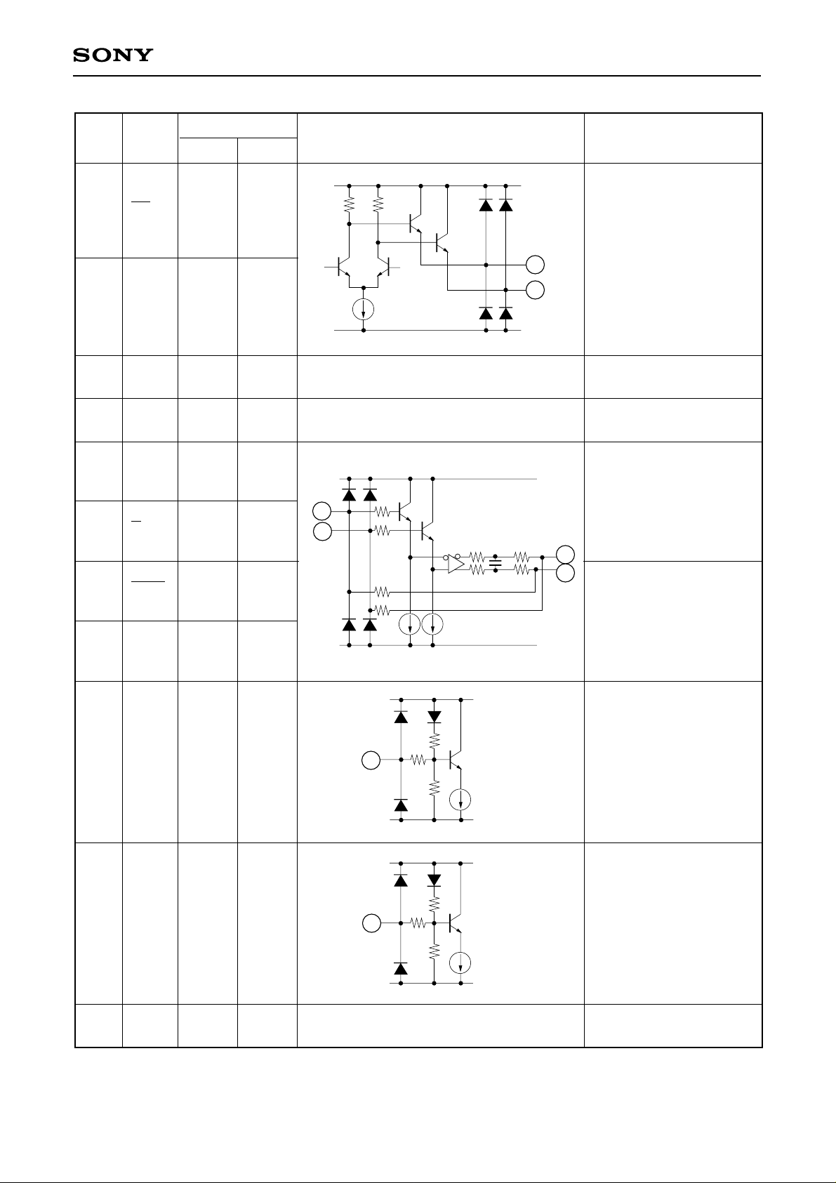
CXB1561Q-Y
Pin
Symbol Equivalent circuit Description
No.
Typical pin voltage
DC AC
CCDA
V
–0.9V
22 CA
—
to
–1.7V
Clock signal output pins.
Terminate these pins in
50Ω at VTT = –2V
Negative power supply
pin for output circuit.
Negative power supply
pin for analog block.
23 CA
24 VEEDA
25 VEEA
—
–5V
–5V
–0.9V
to
–1.7V
22
23
VEEDA
–0.9V
10k
10k
100p
VCCAL
200
200
V
EEA
Post-amplifier input pins.
Ensure that these inputs
are AC-coupled.
28
29
Capacitance connection
pins to determine the
high cut-off frequency for
post-amplifier feedback.
26 D
27 D
28 CAP1
29 CAP1
–1.3V
–1.3V
to
–1.7V
–0.9V
to
–1.7V
26
27
200
200
1k
1k
0.8mA
0.8mA
30 S1
31 S2
–2.0V
–2.0V
32 VccA 0V
30
31
20k
200
50k
20k
200
50k
VCCD
0.1mA
VEED
VCCD
0.1mA
VEED
Delay switchover input pin
for delay block.
∆T = T (S1: High) –
T (S1: open Low)
= 134ps (typ. target)
Pulse width switchover
input pin for differential
circuit.
S2: open low For 622Mbps
S2: High For 155Mbps
Positive power supply pin
for analog block.
– 5 –
CXB1561Q-Y
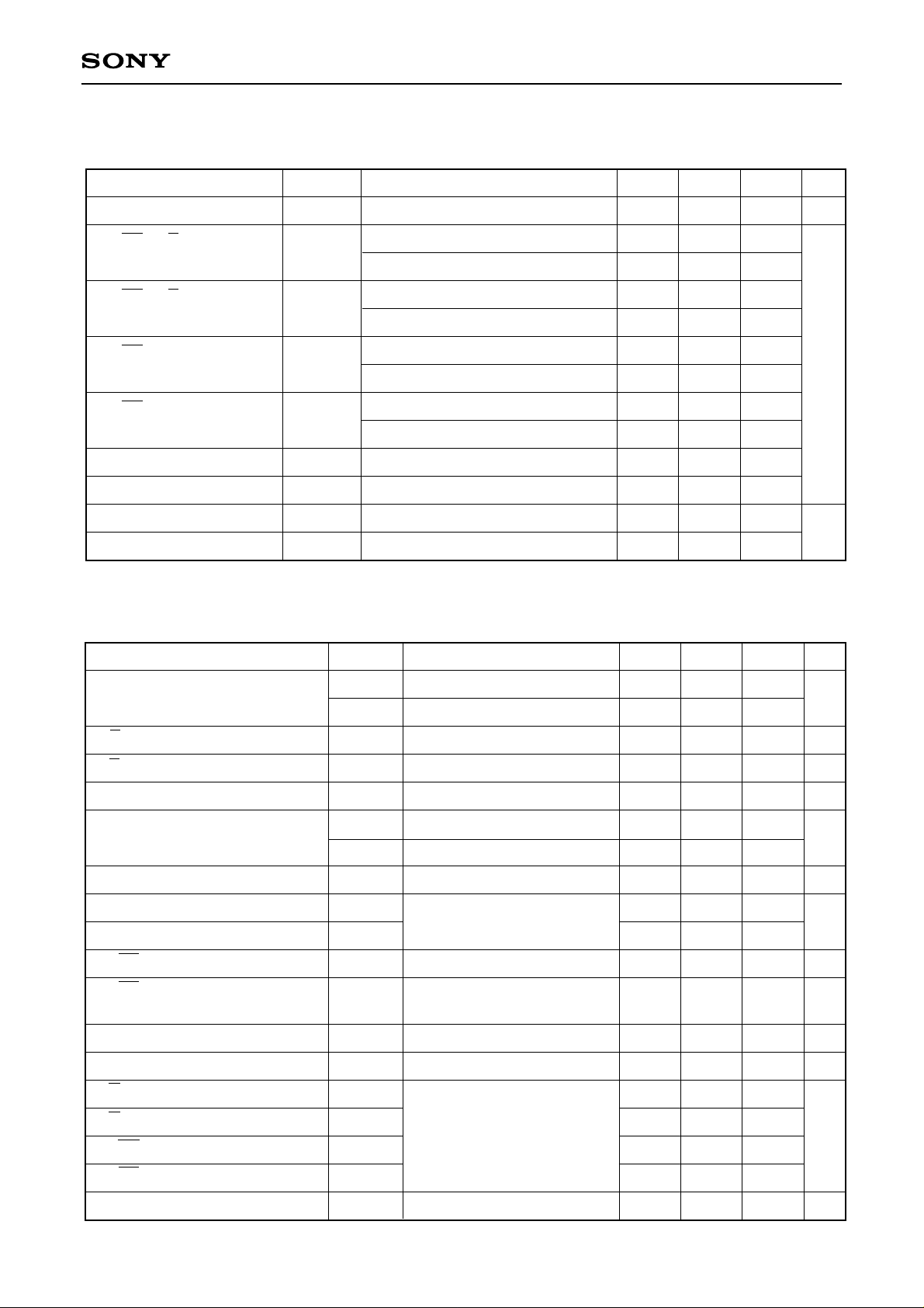
Electrical Characteristics
• DC characteristics (Vcc = 0V, VEE = –5V ± 10%, Tc = –40 to 85°C)
Item
Supply current
CA/CA, Q/Q
High output voltage
CA/CA, Q/Q
Low output voltage
SD/SD
High output voltage
SD/SD
Low output voltage
S1/S2 High input voltage
S1/S2 Low input voltage
S1/S2 High input current
Symbol Conditions Min. Typ. Max. Unit
IEE
Termination: Rt = 50Ω, VTT = –2V
∗1
–157
–1.03
–110 –74
–0.88
mA
VOH-Vcc
Termination: Rt = 50Ω, VTT = –2V
Termination: Rt = 50Ω, VTT = –2V
∗1
–1.15
–1.81
–0.88
–1.62
VOL-Vcc
Termination: Rt = 50Ω, VTT = –2V
Termination: Rt = 510Ω, to VEE
∗1
–1.86
–1.08
–1.60
–0.82
VOHa-Vcc
Termination: Rt = 510Ω, to VEE
Termination: Rt = 510Ω, to VEE
∗1
–1.20
–1.90
–0.83
–1.57
VOLa-Vcc
Termination: Rt = 510Ω, to VEE
VIH-Vcc
VIL-Vcc
IIH
–1.95
–1.17
–3.00
–1.55
0
–1.47
150
V
µA
S1/S2 Low input current
∗1
VEE = –5V, Tc = 0 to 85°C
IIL
–90
• AC characteristics (Vcc = 0V, VEE = –5V ± 10%, VTT = –2V, Tc = –40 to 85°C)
Item
Data rate
D/D input resistance
D/D input identification max. voltage
Post Amp Gain
SQ output pulse width
SQ output amplitude
SQ rise time
SQ fall time
SC/SC input resistance
SC/SC
input identification max
voltage
Limit Amp Gain
Phase margin for the flip-flop block
Q/Q rise time
Symbol Conditions Min. Typ. Max. Unit
Da
S2: open low
414.72
622.08
Mbps
Db
RINM
VmaxM
GP
τd1
S2: High
For single-end input, DC cut-off
I
nternal signal: 400mV
S2: open low
155.52
750
1000
45
525
311.04
1000
760
1250
1075
Ω
mVp-p
dB
ps
τd2
VoB
TrB
TfB
RinL
VinL
GL
∆θ
TrQ
S2: High
Output, DC cut-off, 50Ω load
50Ω load, 20% to 80%
For single-end input, DC cut-off
Internal signal: 400mV
1050
480
200
200
37.5
1000
30
320
200
1625
670
300
300
50
340
440
2150
850
420
400
62.5
650
mV
ps
Ω
mVp-p
dB
deg
Q/Q fall time
CA/CA rise time
CA/CA fall time
CA/CA output duty cycle
TfQ
TrC
TfC
Du
50Ω load, 20% to 80%
– 6 –
200
150
120
45
410
245
215
50
650
350
350
55
ps
%
CXB1561Q-Y
Item
Identification maximum voltage
amplitude of alarm level
Hysteresis width
SD/SD response assert time
SD/SD response deassert time
∗2
CAP2/CAP3 pin capacitance 470pF, V (UP pin) – V (DOWN pin) = 10mV, D input voltage = 130mVp-p
Symbol Conditions Min. Typ. Max. Unit
VmaxA
∆P
Tas
Tdas
D·single-phase input
conversion
∗2
Low → High
High → Low
∗2
∗2
30
2
2.5
6
12
100
100
Electrical Characteristics Measurement Circuit
For DC Characteristics
VTT
mVp-p
dB
µs
50
21
Delay
ALARM
peak hold
peak hold
4
5050
20
delay2
delay1
5
VVVV
23
24
25
DVD
C1R
26
C3
V
C2
V
S1
VS2
VEE
27
28
29
A
30
A
31
32
1
2
A
VUP
3
22
Post
Amp
V
DOWN
50
C6
C4
51
510
510
V
SC
V
V
V
V
19
18
17
Limit Amp
D-FF
6
C8C7
VEEDB
Differential
V
7
EEDB
8
16
15
14
13
12
11
10
9
– 7 –
 Loading...