

Sony CXB1558Q-Y Datasheet
Laser Driver
Description
The CXB1558Q-Y is a high-speed monolithic
Laser Driver/Current Switch with ECL input level.
Open collector outputs are provided at the output
pins (Q, Q) and have the capability of driving
modulation current of 60mApp at a max. data rate of
2.0Gbps (NRZ). DRIVADJ and SDRIV inputs control
the modulation current amplitude, and BIASADJ,
SBIAS inputs control the bias current. Modulation
and bias current can be controlled by either voltage
or current through these pins. This device includes
D-FF for duty cycle correction and Laser Shutdown
function.
Features
• Maximum data rate (NRZ): 2.0Gbps (Typ.)
• Differential Data input: ECL
• D-FF for Duty Cycle Correction
• Laser Shutdown Input: TTL
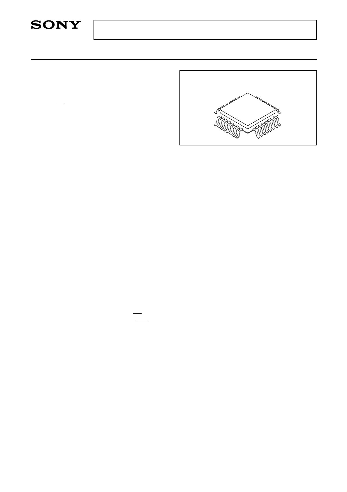
CXB1558Q-Y
32 pin QFP (Ceramic)
Applications
• SONET/SDH: 155,622Mb/s,1.2Gb/s
• Fiber channel: 133,266,532Mb/s,1.062Gb/s
• FDDI: 125Mb/s ESCON: 200Mb/s HDTV: 1.5Gb/s
Absolute Maximum Ratings
• Supply voltage Vcc – VEE –0.3 to +7.0 V
• Input voltage VIN VEE to +0.5 V
• Differential input voltage |VIN – VIN| 0 to 2.5 V
• Differential clock voltage |VCLK – VCLK| 0 to 2.5 V
• Output current (Continuous) IQ, IBIAS 0 to 80 mA
Input current (Continuous) IDRVADJ 0 to 8 mA
IBIASADJ 0 to 8 mA
• Storage temperature Tstg –65 to +150 °C
Recommended Operating Conditions
• DC power supply voltage Vcc – VEE 4.75 to 5.46 V
• Operating case temperature Tc 0 to +85 °C
Structure
Bipolar silicon monolithic IC
Sony reserves the right to change products and specifications without prior notice. This information does not convey any license by
any implication or otherwise under any patents or other right. Application circuits shown, if any, are typical examples illustrating the
operation of the devices. Sony cannot assume responsibility for any problems arising out of the use of these circuits.
– 1 –
E94720-PK
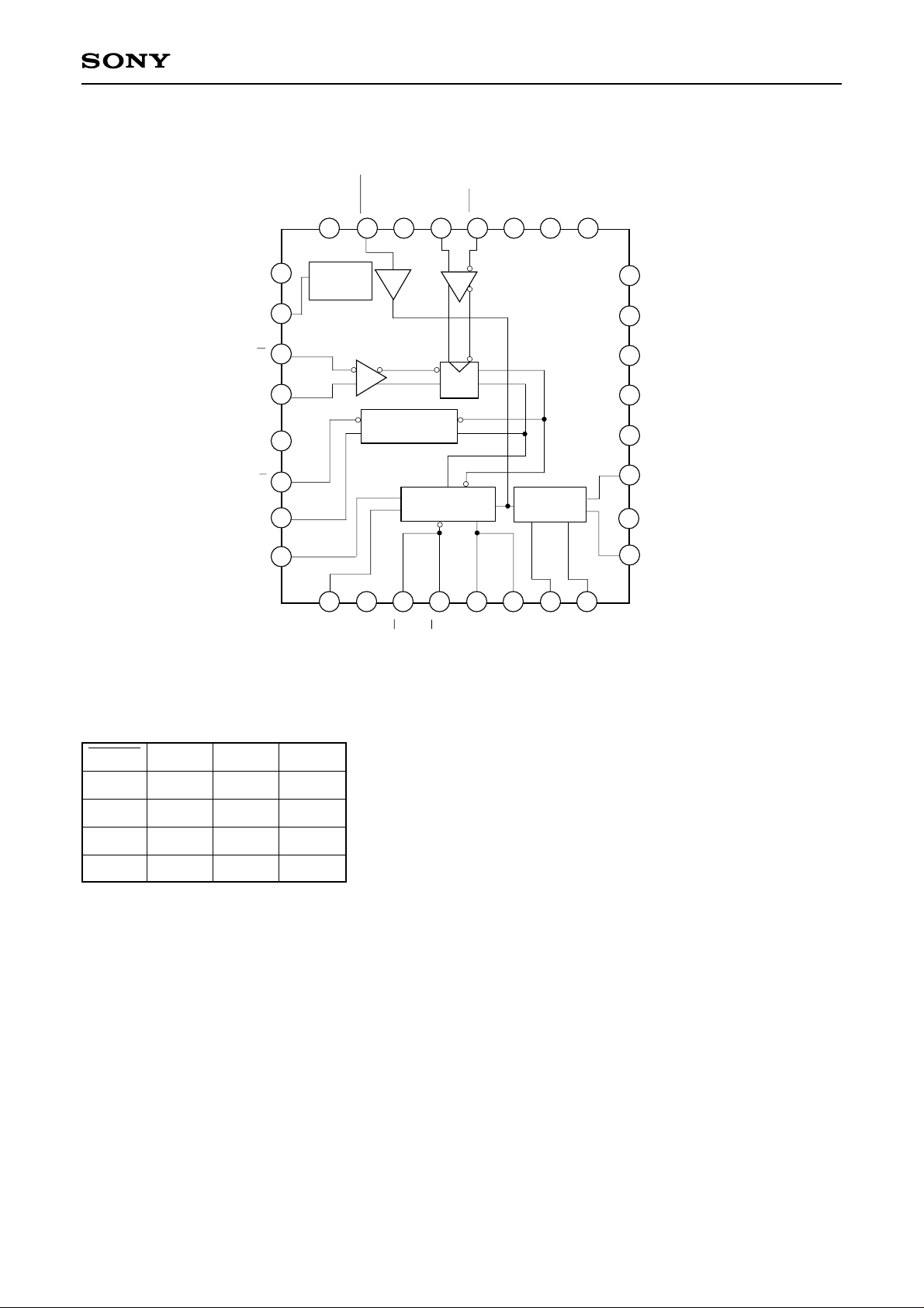
Block Diagram and Pin Assignment
CXB1558Q-Y
EE1
V
V
BB
VCC1
DRIVADJ
2
CC
V
23
24
25
VOLTAGE
SOURCE
26
27
D
D
28
29
30
P
31
P
32
1
SDRIV
NC
LDOFF
22
INPUT SIGNAL
MONITOR
MODULATION
GENERATOR
2
3
2
Q
EE
V
CLK
21
D-FF
4
Q
CLK
20
5
Q
EE
V
NC
19
18
BIAS
GENERATOR
6
7
Q
BIASB
NC
17
8
BIASA
16
15
14
13
12
11
10
9
NC
NC
NC
NC
NC
BIASADJ
VEE2
SBIAS
Truth table
LDOFF
H
H
L
L
∗
In a case of resistor load.
DQP
L
H
L
H
H
L
H
H
H
L
H
L
– 2 –
Pin Description
CXB1558Q-Y
Pin
No.
1
32
2, 10
3
4
5
6
7
Symbol
SDRIV
DRIVADJ
VEE2
Q
Q
BIASB
Typical voltage (V)
DC
AC
0mA to
∗1
8mA
—
0mA to
∗2
6mA
VEE to
VEE +2.5V
–5.2V
0mA to
60mA
—
0mA to
40mA
0mA to
60mA
—
0mA to
40mA
∗1
∗2
∗1
∗2
Equivalent circuit Description
4
3
1
32
2
10 VEE
7
8
Modulation generator
6
5
current monitor.
VCC
Modulation generator
current adjustment.
Negative power supply
pin.
Modulation generator
current output.
8
9
11
20
21
BIASA
SBIAS
BIASADJ
CLK
CLK
0mA to
30mA
0mA to
8mA
VEE to
VEE +2.5V
—
—
—
—
–1.84V to
–0.81V
29
20
21
VCC
9
Bias generator current
output.
Bias generator current
11
monitor.
Bias generator current
2
10
200Ω
200Ω
EE
V
V
adjustment.
CC
Clock signal input.
19
VEE
∗1
VEE = –5.46V to –4.94V
∗2
VEE = –4.94V to –4.75V
–5.2V
—
19
VEE
– 3 –
CXB1558Q-Y
Pin
No.
Symbol
26
VBB —
VEE1—
25
D
27
D
28
Typical voltage (V)
DC
AC
–1.3V
–5.2V
–1.84V to
—
–0.81V
29
27
28
Equivalent circuit Description
V
CC
900Ω
Reference voltage
(–1.3V)
Use for the reference
26
voltage in the case of
single-phase input.
Max. drive current
500µ
VEE
V
±200µA
Negative power supply
CC
pin.
200Ω
200Ω
Data signal input.
29
30
31
VCC1
P
P
0V
—
—
—
0mA to
2.7mA
25
200Ω
30
31
1.7mA
200Ω
VEE
pin.
Input signal monitor
output.
EE
V
Positive power supply
– 4 –
 Loading...