

Sony CXB1549Q Datasheet

CXB1549Q
Laser Diode Driver
Description
The CXB1549Q is a high-speed monolithic Laser
Diode Driver/Current Switch with ECL/PECL input
level. Open collector outputs are provided at the
output pins (Q, QBX) and have the capacity of driving
modulation current of 50mAp-p at a max. data rate of
1.25Gbps (Min.). Along with the modulation current
generator there is the laser diode bias generator
which has capacity of sourcing up to 60mA (Bias).
The laser diode current can be controlled by either a
voltage or current into the bias adjust pin (BiasAdj) and
the bias set pin (SBias), depending on how these
pins are configured. Control of the diode bias current
is achieved through the APC (Automatic Power
Control) circuitry. In order to avoid having a large
current go through the laser diode, this IC also
provides an Activity detector and Power on Reset
functions for Laser Safety. The Activity detector
circuit detects data edge transitions and if no data
transition occur after a certain time period, then both
the modulation and bias current are shutdown.
The Power on Reset circuit holds the modulation
and bias current off for a set period of time while the
system power is applied. Additionally, this IC has an
internal Duty Cycle correction circuit that can control
the falling edge of the input pulse up to a maximum
of 0.2ns (Min.).
Features
• Maximum data rate (NRZ): 1.25Gbps
• Power on Reset function
• Alarm and Shutdown function
• Signal Duty cycle correction
• Automatic Power Control (APC) for bias current
• Activity detector function for laser safety
• Power indicate function
• Differential PECL inputs or AC coupled inputs
Application
• Gbit-ethernet: 1.25Gb/s
• SONET/SDH: 622Mb/s
• Fibre channel: 532Mb/s, 1.062Gb/s
Absolute Maximum Ratings
• Supply voltage Vcc – VEE –0.3 to +6.0 V
• Input voltage VIN VEE to Vcc V
• Differential input voltage
| VD – VDB | 0 to 2.5 V
• Bias output current 0 to 80 mA
• Modulation output current 0 to 70 mA
• SBias input/output current 0 to 5 mA
• Input bias control current
Iset (Ibiasadj) 0 to 5 mA
• Input bias control voltage
Vset (Vbiasadj) 0 to 3 V
• Storage temperature
Tstg –65 to +150 °C
Recommended Operating Conditions
• DC power supply voltage
Vcc – VEE 3.14 to 3.46 V
• Operating ambient temperature
Ta –40 to +85 °C
Structure
Bipolar silicon monolithic IC
– 1 –
E98313B92-PS
Sony reserves the right to change products and specifications without prior notice. This information does not convey any license by
any implication or otherwise under any patents or other right. Application circuits shown, if any, are typical examples illustrating the
operation of the devices. Sony cannot assume responsibility for any problems arising out of the use of these circuits.
40 pin QFP (Plastic)
– 2 –
CXB1549Q
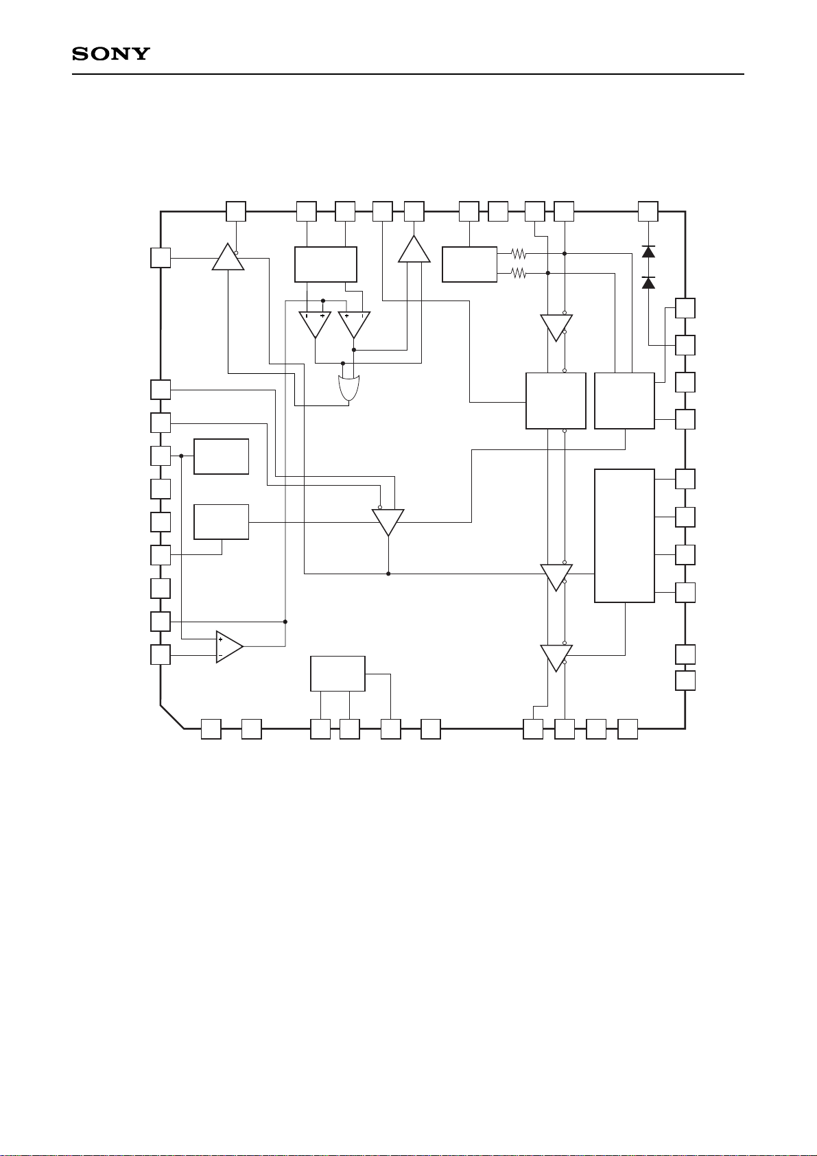
Block Diagram and Pin Assignment
VBB
Generator
VREF
Power on
Reset
Reference
Generator
Bias
Circuit
DRV Cont
In_ALM
35
36
37
34
29 24
RS
28
RSB
27
Tset
26
Indicate
25
VBB
VCC2
D
DB
V
EE2
Q
V
EE5
Bias
SBias
V
CC4
23 22 21
20 ADCDis
16 CompB
15
CompA
19 TM
18 NC
17 Timer
14
DrvAdj
38
V
EE3
CapZ
V
CC3
V
REF
TEST_PIN
SDNB
SDN
LDAlm
39
APCOut
40RsetPD
31
32
33
30
LDAlmB
7
QBX
8
VEE19VEE1
10
DrvMon
11
V
EE1
12
V
CC1
13
6541
VEE4
2
BiasAdj
3
Duty Cycle
Cont
– 3 –
CXB1549Q
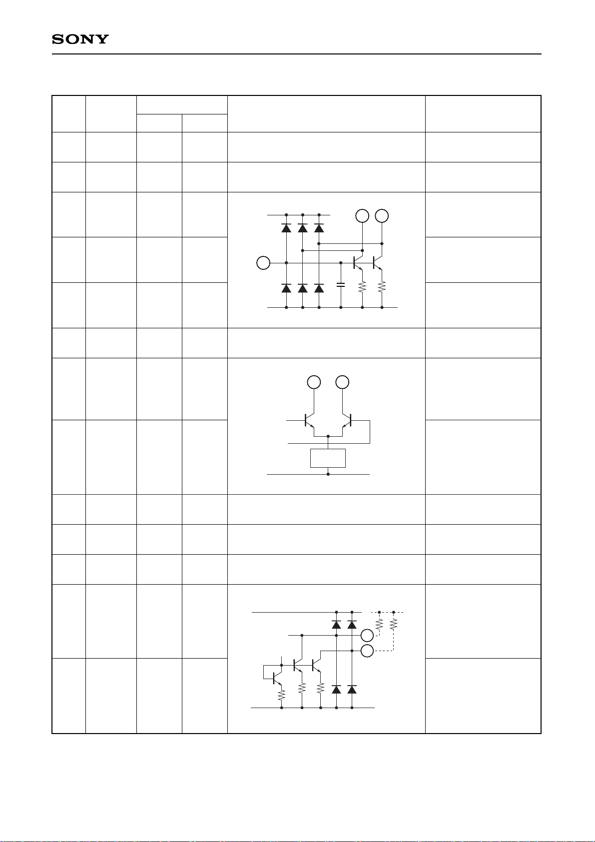
Pin Description
Pad
No.
1 VCC4 3.3
Positive power supply
pin for APC circuit.
2 VEE4 0
Negative power supply
pin for APC circuit.
6 VEE5 0
Negative power supply
pin for Bias circuit.
7 Q 1.3 to 3.3
6mA to
30mA
∗1
6mA to
50mA
∗2
8
QBX
1.3 to 3.3
6mA to
30mA
∗1
6mA to
50mA
∗2
Laser modulation
current output pin.
Open collector output.
9, 10 VEE1 0
Negative power supply
pin for Driver circuit.
11 VCC1 3.3
Positive power supply
pin for Driver circuit.
12 VEE1 0
Negative power supply
pin for Driver circuit.
13
DrvMon
0µA
to
600µA
Sets Laser modulation
current (IQ) monitor pin.
IQ is monitored by
connecting a resistor
(Rmon) to this pin.
14
DrvAdj
0µA
to
600µA
Sets Laser modulation
current pin (IQ).
IQ is controlled by
connecting a resistor
(Rdrv) to this pin.
Refer to Fig.2.
3 BiasAdj
1.5 to 0
Sets Laser bias current
pin.
4 SBias
0mA
to
2.5mA
Sets Laser bias current
or monitor pin.
5 Bias
0mA
to
60mA
Laser bias current
output pin.
Open collector output.
Symbol
Typical voltage [V]
DC AC
Equivalent circuit Description
3
VCC
VEE
10pF
240
30
8
4 5
VEE
7 8
Current
Source
VCC
VEE
1.3k
150
150
Rdrv
Rmon
13
14
∗1
Ta = –40 to 0°C
∗2
Ta = 0 to +85°C
Complementary current
output pin.
Q and QBX are
not symmetrical output.
Use Q output for Laser
modulation.

– 4 –
CXB1549Q
Pad
No.
15 CompA
Modulation current
driver compensation pin.
Normally, connects
180pF Capacitor across
CompA and CompB
pins.
16 CompB
Capacitor port pin for
activity detector
(IN_ALM) operation.
This pin set the period
of inactive time for
activity detector.
Inactive time is
controlled by connecting
a capacitor to this pin.
Refer to Fig.6.
17 Timer
No Connect pin.18 NC
Chip temperature
monitor pin.
19 TM 1.5
This pin control the
activity detector Circuit.
High (connected to Vcc
or open): an activity
detector is disable.
Low (connected to VEE):
an activity detector is
enable.
20 ADCDis
VEE
to
VCC
(open)
Negative power supply
pin for Data input circuit.
21
VEE2 0
Symbol
Typical voltage [V]
DC
AC
Equivalent circuit Description
VCC
VEE
30pF
180pF
10k
15
16
VCC
2.1k
VEE
17
10pF
200µA
Ctimer
25µA
2.4k
2.4k
VEE
19 21
VCC
VEE
3.8k3.8k
15µA
35k
35k
35k
35k
20
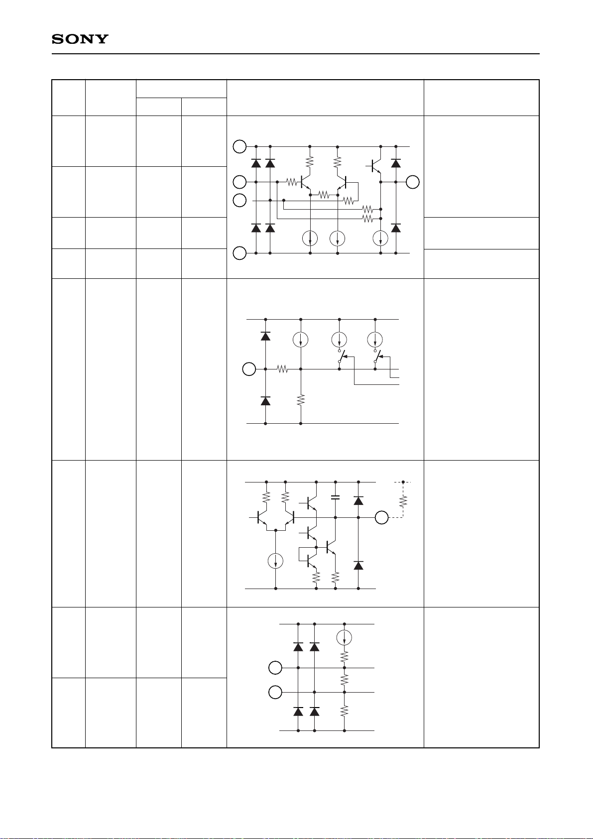
– 5 –
CXB1549Q
Pad
No.
22
DB 1.6 to 2.4
23
D 1.6 to 2.4
24 VCC2 3.3
25 VBB 2
26 Indicate 0.7 to 1.7
Differential PECL data
inputs pins.
These two inputs are
internally biased by
10kΩ to VBB.
Positive power supply
pin for Data input circuit.
Reference bias voltage.
(Option)
The analog voltage high
impedance output pin
which indicate of whether
the optical power of
Laser diode is operated
normal
or not. The power output
range has following
relationship.
High Light Indication;
Vo ≥ 1.7V
Nominal Operation;
Vo = 1.2V
Low Light Indication;
Vo ≤ 0.7V
Symbol
Typical voltage [V]
DC AC
Equivalent circuit Description
24
22 25
21
300
200
200
10k
10k
300
600µA
23
600µA
400
26
100k
V
CC
VEE
14k
50µA
35µA 35µA
27 Tset
Selector for output duty
cycle control pin.
This pin controls the
trailing edge of the input
high pulse. Variable
delay limit of that is from
0 to 0.2ns. Duty cycle is
controlled by connected
a resistor value between
Vcc and this pin.
Refer to Fig.1.
VCC
VEE
Rset
27
2.4k2.4k
20pF
70µA
140220
28 RSB 0.5
29 RS 2.5
Window comparator
top/bottom threshold
voltage pin for
LD_ALARM.
The alarm (fail)
threshold assert voltage
can be set by the
external resistor.
Default voltages are
RS equal to 2.5V and
RSB equal to 0.5V.
29
28
VCC
VEE
100µA
2.5k
20k
5k
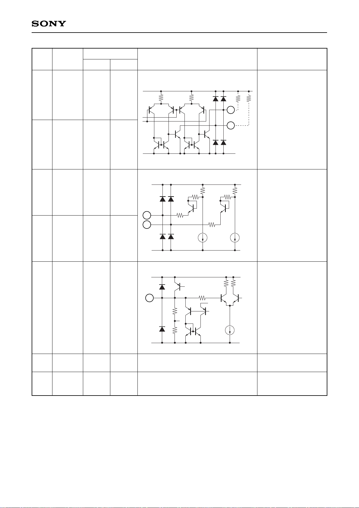
– 6 –
CXB1549Q
Pad
No.
30
LDAlmB 0.2 to 3
31
LDAlm 0.2 to 3
32
SDN 0 to 3.3
33
SDNB 0 to 3.3
34
VREF 1.7
Complementary open
collector TTL outputs.
Asserted when the fault
is detected in the Laser
monitor diode circuit.
Complementary TTL
inputs pin to disable
output current.
(shutdown input)
When left open = "High"
Temperature
compensated reference
voltage pin for APC.
1.7V (Constant for VEE
reference)
Symbol
Typical voltage [V]
DC AC
Equivalent circuit Description
VCC
VEE
4.7k
4.7k
31
30
VCC
VEE
5k
5k
5k
5k
300
300
60µA
60µA
32
33
300300
1.9mA
VCC
VEE
200
34
2.4k
9.1k
35
TEST_
PIN
OPEN
Do not connect.
36
VCC3 3.3
Positive power supply
pin for Signal Detect
circuit.
 Loading...