

Sony CXB1456R Datasheet
VGA/SVGA/XGA 24-bit Receiver
Description
CXB1456R is the 1 chip deserializer for VGA/SVGA/
XGA 24-bit color digital RGB, and meet to the Gigabit
Video Interface specification.
Features
• 1 chip receiver for serial transmission of 24-bit color
VGA/SVGA/XGA picture
• On chip PLL circuit for data and clock recovery
• On chip panel mode automatically selectable circuit
• TTL compatible I/O
• Support 1 pixel/shiftclock mode with 1 chip and 2
pixel/shiftclock mode with 2 chip
• +3.3V single power supply
• Low power consumption
• 64pin plastic LQFP package with body size 10mm
× 10mm
Application
Gigabit video interface
Structure
Bi-CMOS IC
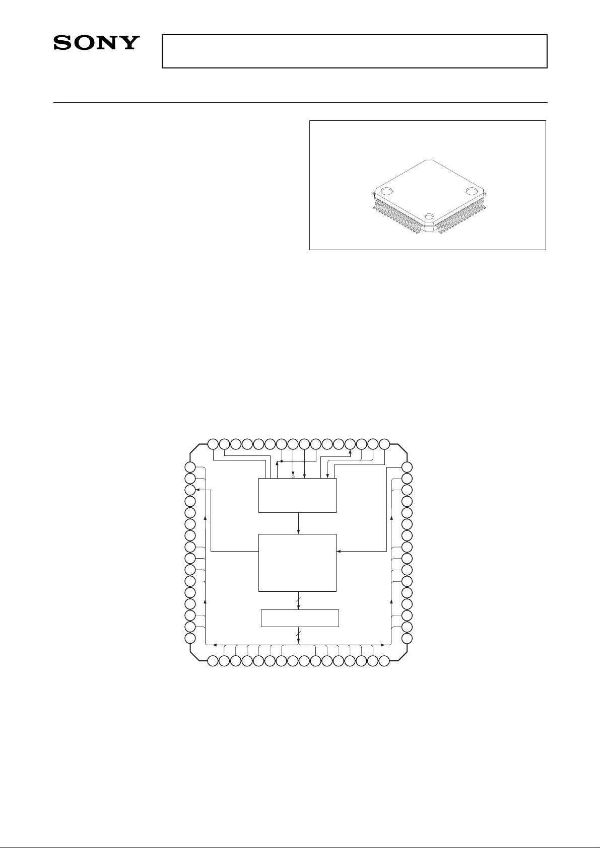
Block Digagram & Pin out
Absolute Maximum Ratings
• Supply voltage Vcc 4.2 V
• Storage temperature Tstg –65 to +150 °C
• Allowable power dissipation
PD 650 mW
Recommended Operating Condition
• Supply voltage 3.3 ± 0.3 V
• Operating temperature Topr 0 to +80 °C
– 1 –
E98Y04C9X-PS
Sony reserves the right to change products and specifications without prior notice. This information does not convey any license by
any implication or otherwise under any patents or other right. Application circuits shown, if any, are typical examples illustrating the
operation of the devices. Sony cannot assume responsibility for any problems arising out of the use of these circuits.
CXB1456R
64 pin LQFP (Plastic)
49
50
51
52
53
54
55
56
57
58
59
60
61
62
63
64
1
2
3
4 5 6 7 8 9 10 11 12 13 14 15 16
17
18
19
20
21
22
23
24
25
26
27
28
29
30
31
32
33
34
35
36373839404142434445464748
REXT
PANEL0
PANEL1
LOS
TESTDT
CE
REFRQP
SDATAP
SDATAN
REFRQN
TESTEXN
V
CCAVEEAVEES
LPFA
LPFB
V
DD
G0
G1
G2
G3
G4
G5
GND
V
DD
G6
G7
B0
B1
B2
B3
GND
CLKPOL
R0
R1
GND
V
DD
VEE
VCC
R2
R3
R4
R5
GND
V
DD
R6
R7
GND
CNTL
DE
SFTCLK
GND
V
DD
VEE
VCC
HSYNC
VSYNC
B7
B6
GND
V
DD
B5
B4
V
DD
Serial
to
Parallel
Converter
Decoder
CDR
PLL
Fig. 1. Block Diagram & Pin out
– 2 –
CXB1456R
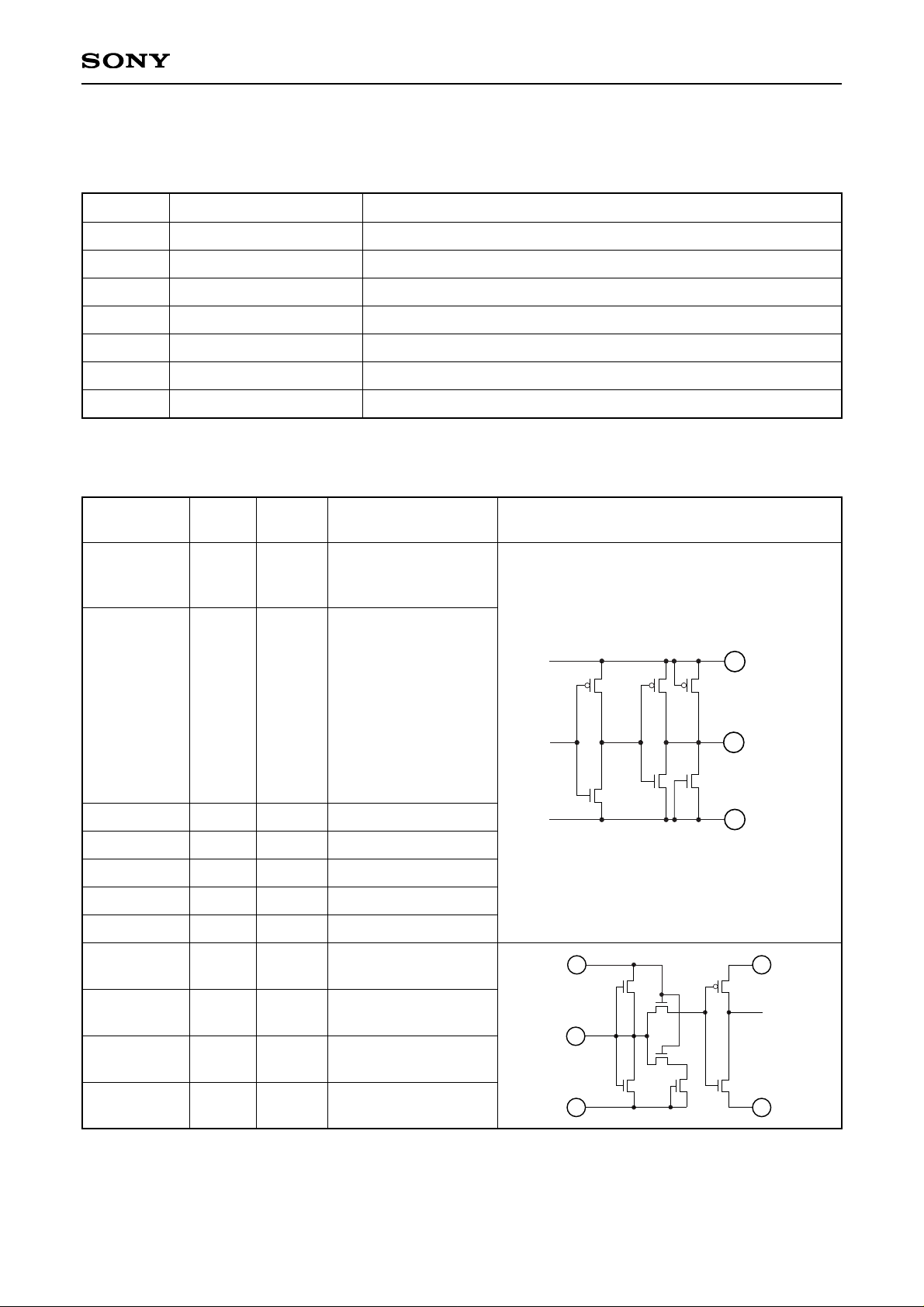
Pin List
Table 1. Power/Ground
Pin name
VDD
GND
VCC
VEE
VCCA
VEEA
VEES
8, 16, 20, 28, 53, 61, 64
1, 9, 17, 21, 29, 52, 60
26, 55
27, 54
44
45
46
MOS power supply, should be connected to 3.3V ± 0.3V
MOS ground, connected to 0V
ECL power supply, connected to 3.3V ± 0.3V
ECL ground, connected to 0V
Analog power supply, connected to 3.3V ± 0.3V
Analog ground, connected to 0V
Substrate GND, connected to 0V
Pin number Descriptions
Table 2. Digital Signals
Pin name
SFTCLK
RED (7 to 0)
GRN (7 to 0)
BLU (7 to 0)
HSYNC
VSYNC
CNTL
DE
LOS
PANEL (1, 0)
CLKPOL
CE
TESTEXN
TESTDT
51
18, 19,
22, 23,
24, 25,
30, 31
6, 7, 10,
11, 12,
13, 14, 15
58, 59,
62, 63,
2, 3, 4, 5
56
57
49
50
36
35, 34
32
38
43,
37
TTL out
TTL out
TTL out
TTL out
TTL out
TTL out
TTL out
TTL in
TTL in
TTL in
TTL in
Shift clock, for the
data fetch at falling or
rising edge
Pixel data
Hsync data
Vsync data
Control data
Display enable data
Los of signal
Panel mode select
switch
Trigger edge select
switch
Chip enable
Reversed for TEST
under fabrication
Pin
number
Type
Descriptions Equivalent circuit
VDD
GND
V
CCA
TTL-IN
V
EES
VDD
TTL-OUT
GND
– 3 –
CXB1456R
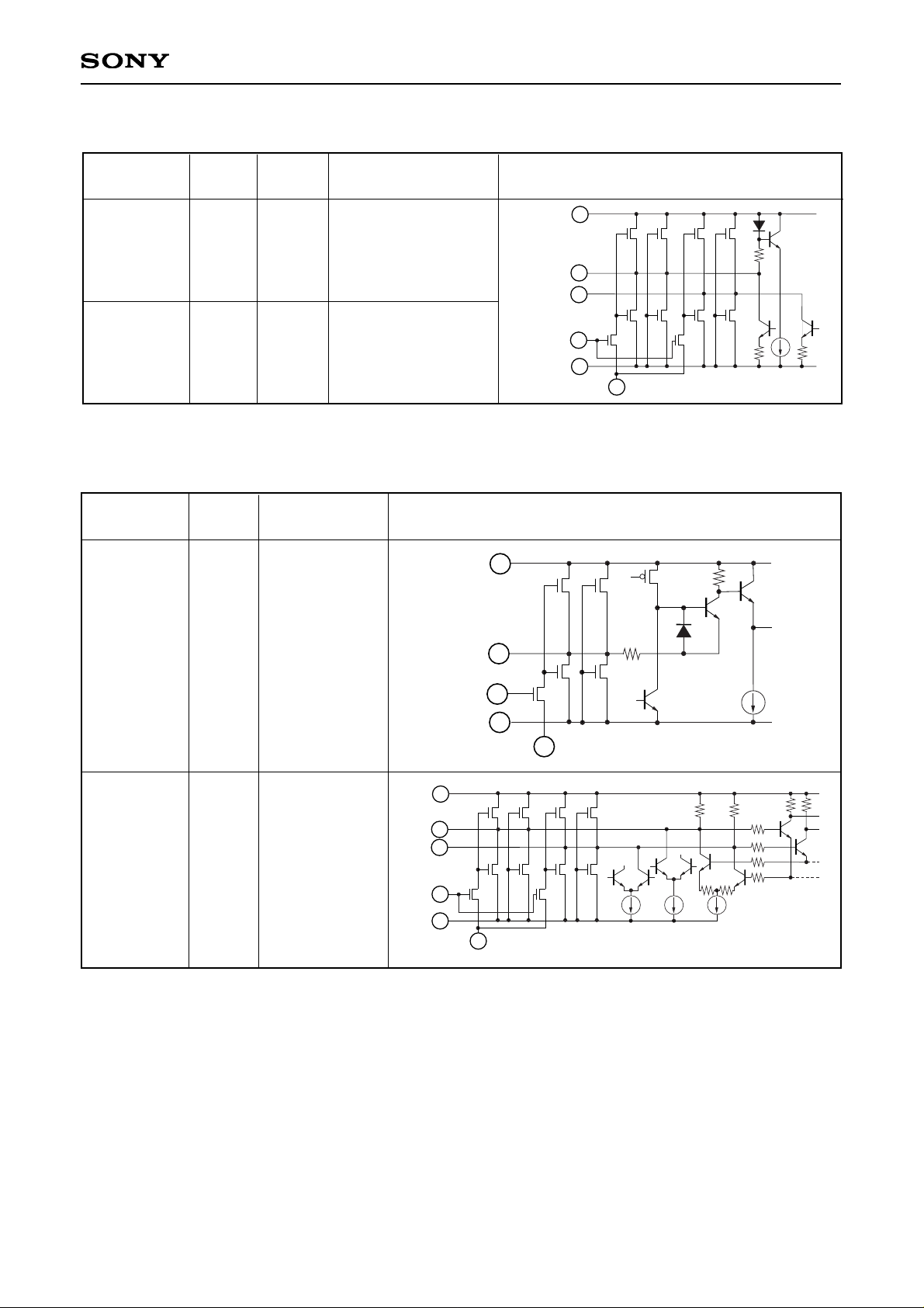
Table 3. Special
Pin name
33
47, 48
External Register
External loop
filter
Pin
number
Descriptions
Equivalent circuit
REXT
LPFA/B
Table 2. Digital Signals (Cont.)
Pin name
SDATAP/N
REFRQP/N
40, 41
39, 42RxRx
Serial input
Refclk request
Pin
number
Type Descriptions Equivalent circuit
VCCA
SDATAP/N
V
EEA
REFRQP/N
VDD
GND
VCCA
LPFA
V
EEA
VDD
GND
LPFB
VCC
VEE
GND
REXT
VDD
– 4 –
CXB1456R
Electrical characteristics
Table 4. Absolute Maximum Rating
Description
Power supply voltage
TTL DC input voltage
TTL output current (High)
TTL output current (Low)
Serial input pin voltage
REFREQ output pin voltage
Storage temperature
VCC
VI_T
IOH_T
IOL_T
Vsdin
VRQout
Tstg
–0.3
–0.5
–10
0
–0.5
0.5
–65
4.2
4.6
0
10
VCC + 0.5
VCC + 0.5
150
V
V
mA
'
mA
V
V
°C
Symbol Min. Typ. Max. Unit Comments
Table 5. Recommended Operating Conditions
Description
Power supply voltage
Ambient temperature
VCC
Ta
3.0
0
3.3 3.6
80
V
°C
Symbol Min. Typ. Max. Unit Comments
Table 6. DC Characteristics (Under the recommended conditons. See Tab. 5)
Description
Input HIGH voltage (TTL)
Input LOW voltage (TTL)
Input HIGH current (TTL)
Input LOW current (TTL)
Output HIGH voltage (TTL)
Output LOW voltage (TTL)
Output HIGH current (REFREQ)
Output LOW current (REFREQ)
Input dynamic range (SDATA)
Input dynamic range (SDATA)
Supply current
VIH_T
VIL_T
IIH_T
IIL_T
VOH_T
VOL_T
IOH_RQ
IOL_RQ
VIM_SD
VID_SD
ICC
2
0
–10
2.4
–0.1
7.8
VCC – 0.4
–0.5
0
138
77
VCC
0.8
10
0.4
+0.1
11
VCC + 0.2
+0.5
173
104
V
V
µA
µA
V
V
mA
mA
V
V
mA
mA
VIN = VCC
VIN = 0
IOH = –3mA
IOL = 3mA
See Fig. 3, 4
REXT = 5.6kΩ
Common mode voltage
Differential voltage
CL = 8pF, f = 65MHz
See Fig. 9, 10
Symbol Min. Typ. Max. Unit Conditions
Worst Case
16 Grayscale
– 5 –
CXB1456R
37
38
43
39
42
TESTDT
CXB1456R
V
CC
CE
TESTEXN
REFRQP
150Ω
50Ω
50Ω
150Ω
REFRQN
VDD/VCC/VCCA
GND/V
EE/VEEA
A A
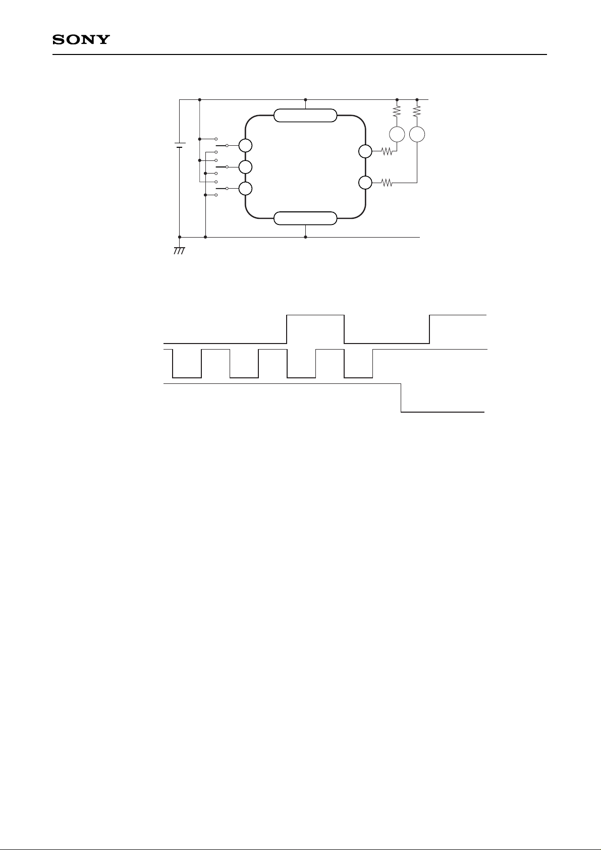
Fig. 3. IOH_RQ and IOL_RQ DC measurement
TESTDT
CE
TESTEXN
Fig. 4. IOH_RQ and IOL_RQ DC measurement setting
– 6 –
CXB1456R
Table 7. AC Characteristics (Under the recommended conditons. See Tab. 5)
Description
Minimum SFTCLK frequency
Maximum SFTCLK frequency
SFTCLK duty factor
Pixel/Sync/Cntl/DE setup to
SFTCLK
Pixel/Sync/Cntl/DE hold to
SFTCLK
SFTCLK rise time
SFTCLK fall time
Pixel/Sync/Cntl/DE rise time
Pixel/Sync/Cntl/DE fall time
CLOCK mode assert time
CLOCK mode deassert time
LOS signal assert time
LOS signal deassert time
Fsftclk
Dsftclk
Tsetup
Thold
Torc
Tofc
Tord
Tord
TAclk
TDclk
TAlos
TDlos
65.0
35
17
9
4.5
16
9
4.5
0.5
20
0.5
0.15
25.0
65
5
3
5
3
MHz
MHz
%
ns
ns
ns
ns
ns
ns
ns
ns
ns
ns
µs
µs
µs
µs
Vth = 1.4V, CL = 8pF
Vth = 1.4V, CL = 8pF
25MHz
40MHz
65MHz
Vth = 1.4V, CL = 8pF
25MHz
40MHz
65MHz
0.8V to 2.0V, CL = 8pF
2.0V to 0.8V, CL = 8pF
0.8V to 2.0V, CL = 8pF
2.0V to 0.8V, CL = 8pF
Symbol Min. Typ. Max. Unit Conditions
CXB1456R
TTLout
Cprobe
CL' + Cprobe = 8pF
oscilloscope
V
CC
CL'
VDD/VCC/VCCA
GND/V
EE/VEEA
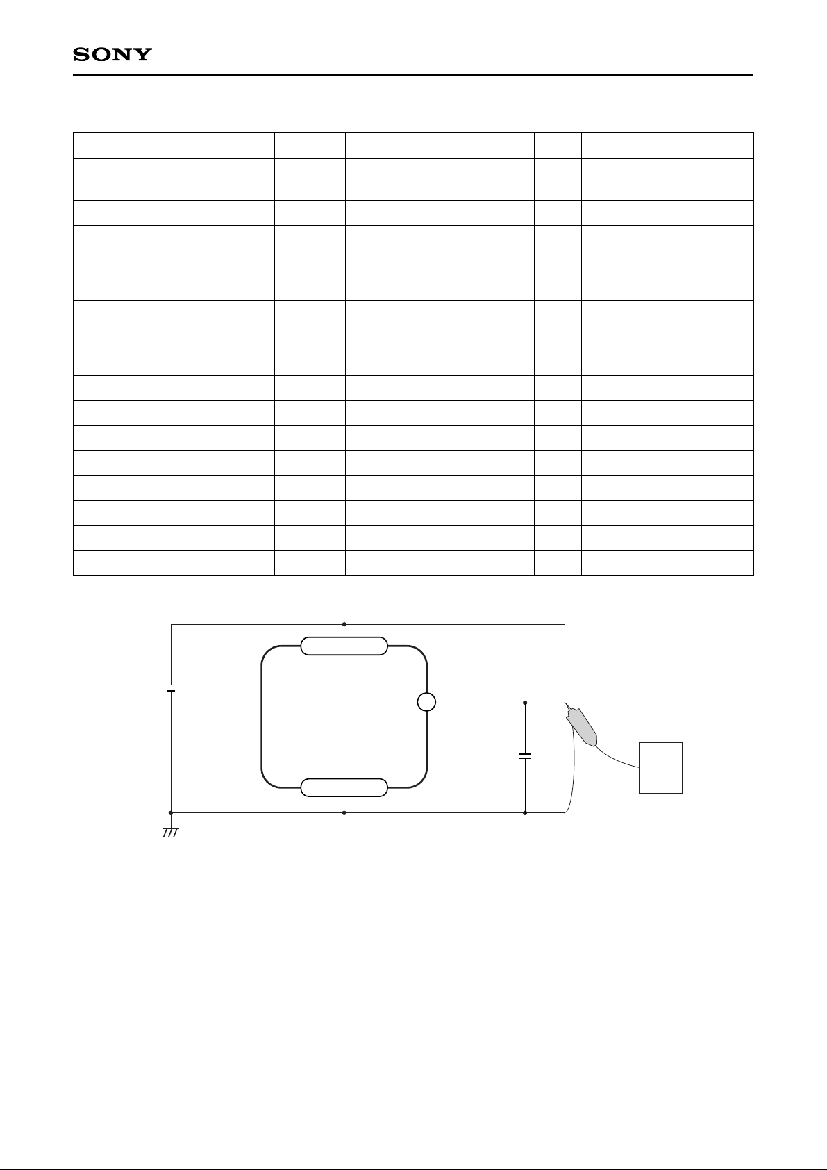
Fig. 5. Pixel/Sync/Cntl/DE waveform measurement
 Loading...