

Sony CXB1452Q Datasheet
VGA/SVGA/XGA digital data serial receiver
Features
• 1 chip receiver for serial transmission of 18bit color
VGA/SVGA/XGA picture
• On chip differential cable driver
• TTL/CMOS compatible interface
• Support 1 pixel/shiftclock mode & 2 pixel/shiftclock
mode
• +3.3V single power supply
• Low power consumption
• 80pin Plastic QFP Package
(Body size: 14mm × 14mm)
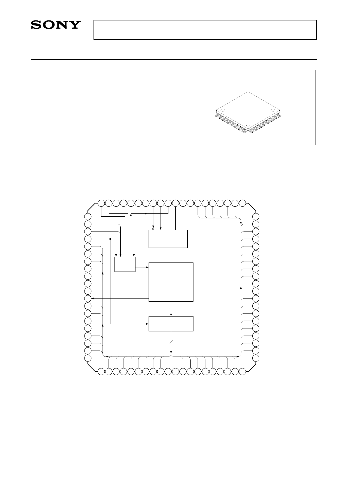
Block Digagram & Pin out
LOS
49
T
T
CC
EE
V
V
RED0 (0)
46
48
47
60
LPFB
59
LPFA
58
A
A
S
CC
EE
EE
V
V
57
56
V
55
REFRQN
TESTSB
53
54
SDATAP
SDATAN
52
51
REFRQP
50
CXB1452Q
80 pin QFP (Plastic)
T
EE
RED0 (4)
RED0 (3)
RED0 (2)
RED0 (1)
45
44
43
RED0 (5)
41
42
V
TESTDT
PANEL1
PANEL0
CKMODE
CNTL3
CNTL2
CNTL1
V
EEG
CCG
V
CCT
V
EET
V
SFTCLK
HSYNC
VSYNC
EEG
V
CCG
V
CNTL0
BLU1 (5)
BLU1 (4)
CCT
V
61
62
63
64
65
66
67
68
69
70
71
72
73
74
75
76
77
78
79
80
1
T
EE
V
2
3
BLU1 (3)
CDR
PLL
4
BLU1 (1)
BLU1 (2)
6
5
BLU1 (0)
8
7
GRN1 (5)
GRN1 (4)
Cable
EQ
Serial
Parallell
Converter
Decoder
9
10
GRN1 (2)
GRN1 (3)
40
CCT
V
GRN0 (0)
39
38
GRN0 (1)
37
GRN0 (2)
36
GRN0 (3)
35
GRN0 (4)
GRN0 (5)
34
33
EEG
V
32
CCG
to
13
12
14
15
11
T
T
EE
CC
V
V
GRN1 (0)
GRN1 (1)
16
RED1 (4)
RED1 (5)
RED1 (3)
18
17
RED1 (2)
19
20
RED1 (0)
RED1 (1)
T
CC
V
31
30
29
28
27
26
25
24
23
22
21
V
EET
V
VCCT
BLU0 (0)
BLU0 (1)
BLU0 (2)
EEG
V
CCG
V
BLU0 (3)
BLU0 (4)
BLU0 (5)
EET
V
Fig. 1. Block Diagram & Pin out
Sony reserves the right to change products and specifications without prior notice. This information does not convey any license by
any implication or otherwise under any patents or other right. Application circuits shown, if any, are typical examples illustrating the
operation of the devices. Sony cannot assume responsibility for any problems arising out of the use of these circuits.
– 1 –
E97937-PS

Pin List
Power/Ground
CXB1452Q
Pin Name
VCCT
VEET
VCCG
VEEG
VCCA
VEEA
VEES
Digital Signals
Pin Name
SFTCLK
RED1 (5 to 0)
GRN1 (5 to 0)
BLU1 (5 to 0)
RED0 (5 to 0)
GRN0 (5 to 0)
BLU0 (5 to 0)
Pin Number Descriptions
10, 20, 30, 40, 48, 70, 80
1, 11, 21, 31, 41, 49, 71
25, 32, 69, 76
26, 33, 68, 75
56
57
58
Pin Number Type Descriptions
72
14, 15, 16, 17, 18, 19
6, 7, 8, 9, 12, 13
78, 79, 2, 3, 4, 5
42, 43, 44, 45, 46, 47
34, 35, 36, 37, 38, 39
22, 23, 24, 27, 28, 29
TTL power surpply , should be connected to 3.3V ± 5%
TTL ground, connected to 0V
Logical core power surpply, connected to 3.3V ± 5%
Logical core ground, connected to 0V
Analog power surpply, connected to 3.3V ± 5%
Analog ground, connected to 0V
Analog substrate, connected to 0V
TTL out
TTL out
TTL out
Shift clock, for the data fetch at falling or rising edge
Pixel data input in 1 pixcel/sftclk mode
2nd pixel data input in 2 pixel/sftclk mode
High fixed in 1 pixcel/sftclk mode
1st pixel data input in 2 pixel/sftclk mode
HSYNC
VSYNC
CNTL (3 to 0)
PANEL (1, 0)
CKMODE
LOS
SDATAP/N
REFRQP/N
Special
Pin Name
TESTSB/DT
LPFA/B
73
74
65, 66, 67, 77
62, 63
64
50
52, 53
51, 54
TTL out
TTL out
TTL out
TTL in
TTL in
TTL out
Rx
Rx
Hsync data
Vsync data
Control data
Panel mode select switch
Clock mode select switch
Los of signal
Serial input
Refclk request
Pin Number Descriptions
55, 61
59, 60
Polarity control of SFTCLK & TEST under fablication
External loop filter
– 2 –
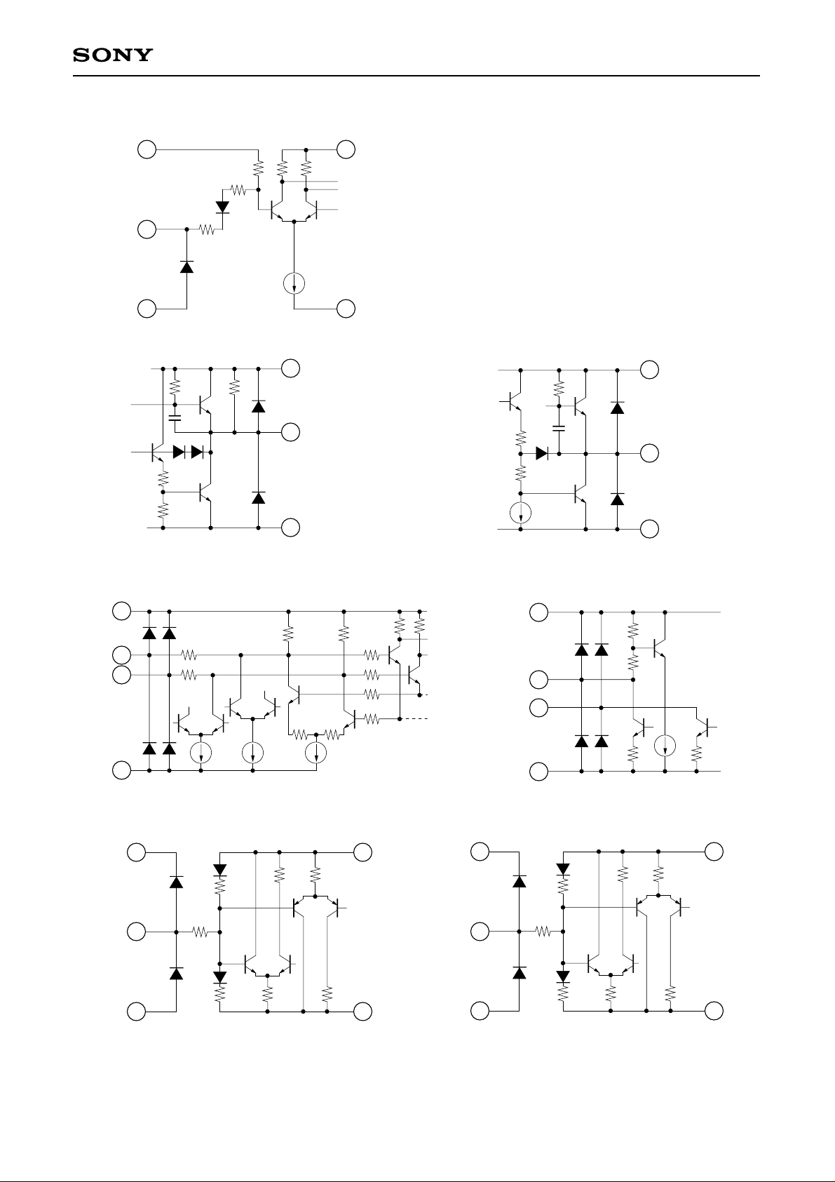
Equivalent I/O circuit
CXB1452Q
VCCT
6k
6k
TTL-IN
300
VEET
(a) TTL input equivalent circuit
3k
(b) TTL output equivalent circuit
SFTCLK, LOS
VCCT
TTL-OUT
V
EET
VCCG
V
EEG
VCCT
TTL-OUT
V
EET
(b') TTL output equivalent circuit
REDxx, GRNxx, BLUxx, H/V sync, CNTLx
VCCA
LPFA
LPFB
EEA
V
VCCA
TESTDT
EEA
V
VCCG
SDATAP/N
REFRQP/N
EEG
V
(c) LPFA/B equivalent circuit (d) SDATAP/N REFRQP/N equivalent circuit
V
V
CCG
EEG
VCCT
TESTSB
EETVEEG
V
V
CCG
(e) TESTDT equivalent circuit (f) TESTSB equivalent circuit
– 3 –
Electrical characteristics
Tab. 1. Absolute Maximum Rating
CXB1452Q
Description
Power supply voltage
TTL DC input voltage
TTL output current (High)
TTL output current (Low)
Serial output pin voltage
Ambient temperature
Storage temperature
Symbol Min. Typ. Max. Unit Comments
VCC
VI_T
IOH_T
IOL_T
Vsdout
Ta
Tstg
–0.3
–0.5
–20
0
–0.5
–55
–65
4
5.5
0
20
VCC + 0.5
60
150
Tab. 2. Recommended Operating Conditions
Description
Power supply voltage (Include VCCT5)
Ambient temperature
Symbol Min. Typ. Max. Unit Comments
VCC
Ta
3.135
0
3.3 3.465
60
Tab. 3. DC Characteristics (Under the recommended conditons. See Tab. 2)
V
V
mA
'
mA
V
°C°CUnder bias
V
°C
Description
Input HIGH voltage (TTL)
Input LOW voltage (TTL)
Input HIGH current (TTL)
Input LOW current (TTL)
Output HIGH voltage (TTL)
Output LOW voltage (TTL)
Output HIGH current (REFREQ)
Output LOW current (REFREQ)
Input dynamic range (SDATA)
Input dynamic range (SDATA)
Supply current
Symbol Min. Typ. Max. Unit Conditions
VIH_T
VIL_T
IIH_T
IIL_T
VOH_T
VOL_T
IOH_RQ
2
–0.5
–400
2.25
–0.1
5.5
0.8
20
0.4
0
+0.1
V
V
µA
µA
V
V
mA
VIN = VCC
VIN = 0
IOH = –0.2mA
IOL = 4mA
See Fig. 2
IOL_RQ
VIM_SD
VID_SD
ICC
7.4
VCC – 0.4
–0.5
230
220
8.0
310
300
8.6
VCC + 0.2
+0.5
390
380
mA
V
V
mA
mA
Common mode voltage
Differential voltage
2 pixel/sftclk, Outputs open
1 pixel/sftclk, Outputs open
– 4 –
 Loading...