


LCD Driver
Description
The CXA7000R is a driver IC developed for use
with Sony polycrystalline silicon TFT LCD panels. It
supports 10-bit digital input, and the input data is
analog demultiplexed into 6 phases and output. The
CXA7000R can directly drive an LCD panel, and the
VCOM setting circuit and precharge pulse waveform
generator are also on-chip.
Features
• Supports 10-bit input
• Supports signals up to XGA
• Low output deviation by on-chip output offset cancel circuit
• On-chip timing generator with ECL
• VCOM voltage generation circuit
• Precharge pulse waveform generation circuit
CXA7000R
64 pin LQFP (Plastic)
Applications
LCD projectors and other video equipment
Absolute Maximum Ratings (VSS = 0V)
• Supply voltage VCC 16 V
VDD 5.5 V
• Operating temperature Topr –20 to +70 °C
• Storage temperature Tstg –65 to +150 °C
• Allowable power dissipation PD 1250 mW
Recommended Operating Conditions
• Supply voltage VCC 15.0 to 15.5 V
VDD 4.75 to 5.25 V
• Operating temperature Topr –20 to +70 °C
Sony reserves the right to change products and specifications without prior notice. This information does not convey any license by
any implication or otherwise under any patents or other right. Application circuits shown, if any, are typical examples illustrating the
operation of the devices. Sony cannot assume responsibility for any problems arising out of the use of these circuits.
– 1 –
E01821A22
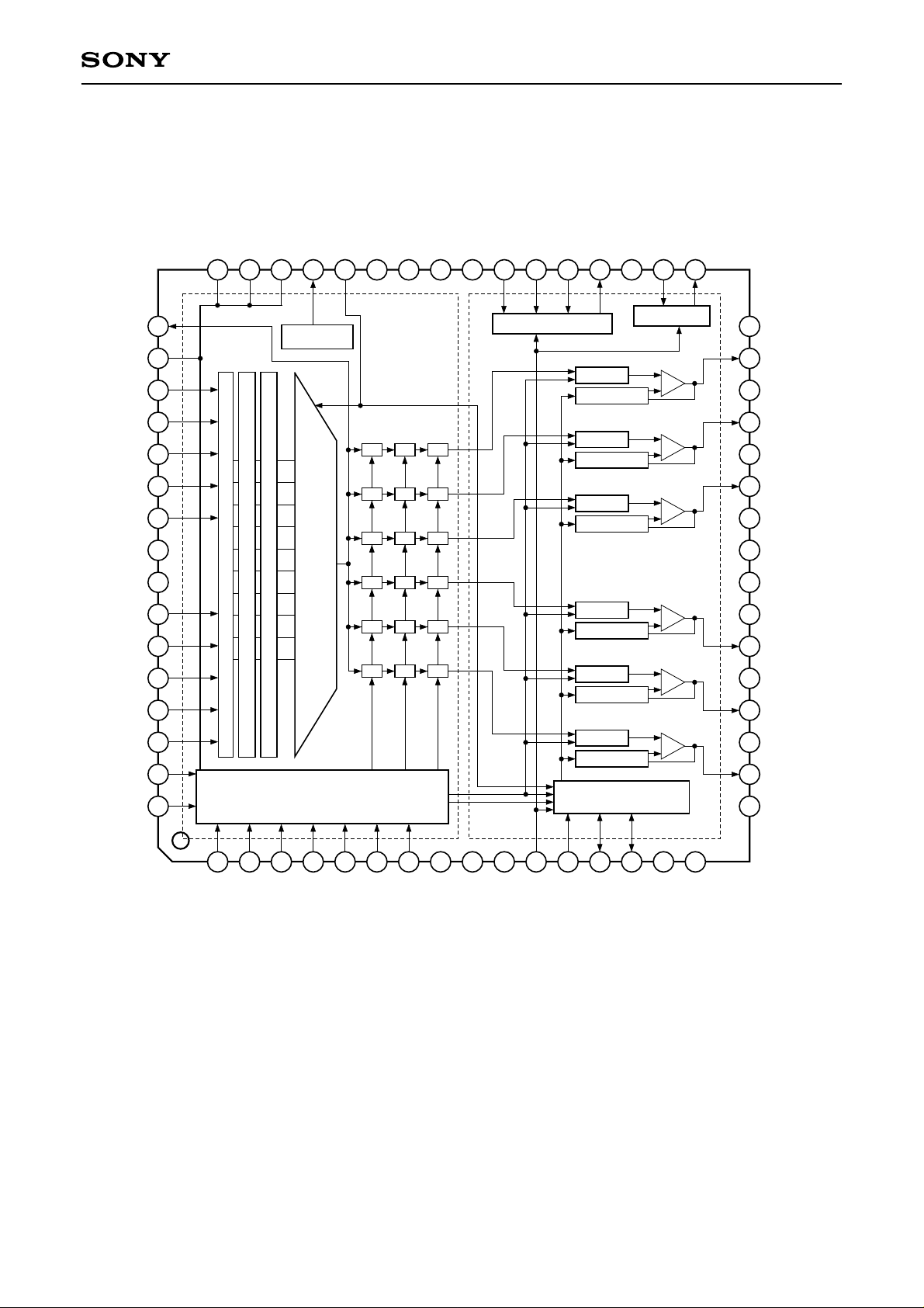
Block Diagram
CXA7000R
TEST
STATUS
D_IN9
D_IN8
D_IN7
D_IN6
D_IN5
GND
GND
D_IN4
D_IN3
D_IN2
D_IN1
49
50
51
52
53
54
55
56
57
58
59
60
61
VREF_I
VREF_O
F/H_CNT
DIRC
SL_DAT
48 47 46 45 44 43
Vref Gen.
S/H S/H S/H
S/H S/H S/H
S/H S/H S/H
D/A
S/H S/H S/H
S/H S/H S/H
S/H S/H S/H
5
DD
V
PS
42
GND
GND
41 40 39 38 37
PRG
SID_Gen.
SID_LV
SID_OUT
PRG_LV
36
Line inv.
Offset Cancel
Line inv.
Offset Cancel
Line inv.
Offset Cancel
Line inv.
Offset Cancel
Line inv.
Offset Cancel
15
CC
VCOM_OFST
V
35 34 33
VCOM_Gen.
VCOM_OUT
32
31
30
29
28
27
26
25
24
23
22
21
20
PV
CC
SH_OUT1
NC
SH_OUT2
NC
SH_OUT3
GND
PGND
PGND
GND
SH_OUT4
NC
SH_OUT5
D_IN0
MCLK
MCLKX
62
63
64
TG
1 2 3 4 5 6
FRP
SHST
POSCNT2
POSCNT1
POSCNT0
FRP
CAL_PLS
7
SHTEST
POSCNT3
8 9 10 11 12
GND
SIG.C
NC
GND
– 2 –
Line inv.
Offset Cancel
Offset Cancel Control
13
14 15 16
CAL_L
GND
CAL_H
SIG_OFST
19
18
17
DCFBOFF
NC
SH_OUT6
CC
PV
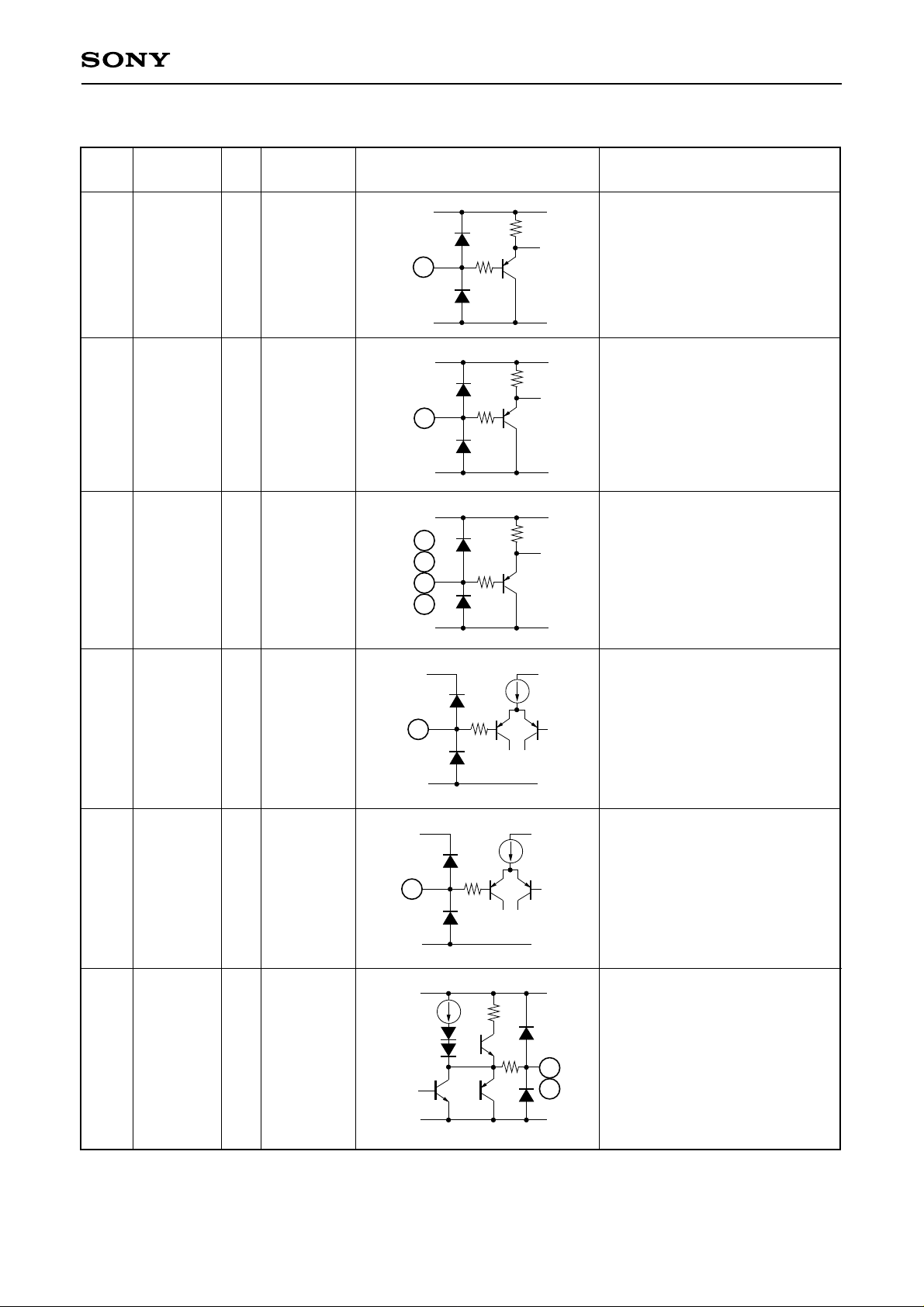
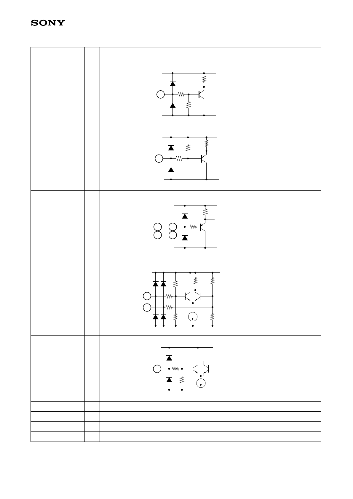
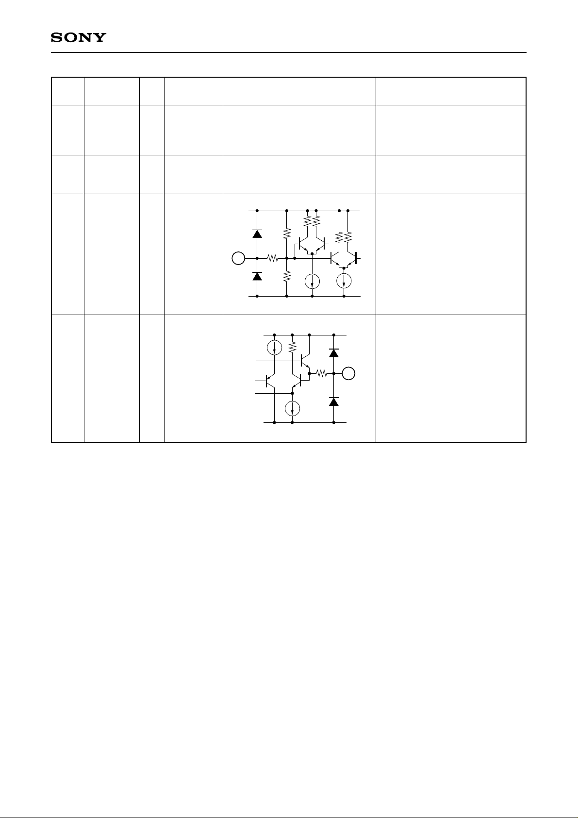
Pin Description
CXA7000R
Pin
No.
3
4
5
6
Symbol I/O
POSCNT0
POSCNT1
POSCNT2
POSCNT3
Standard
voltage level
High: ≥2.0V
IFRP1
Low: ≤0.8V
High: ≥2.0V
ISHST2
Low: ≤0.8V
High: ≥2.0V
I
Low: ≤0.8V
Equivalent circuit Description
V
DD
50k
192
1
LCD panel AC drive inversion
timing input.
High: inverted
Low: non-inverted
See the Timing Chart.
GND
V
DD
50k
2
192
Internal sample-and-hold timing
circuit reset pulse input.
This pin is also used as the
offset cancel level insertion
timing input.
A reset is applied to the internal
timing generator at the falling
GND
V
DD
GND
3
4
5
6
192
50k
edge.
Output phase adjustment.
The output phase is adjusted in
MCLK period units when
SL_DAT is high, and in
1/2 MCLK period units when
SL_DAT is low.
13
14
CAL_L
CAL_H
ISIG.C11
I/O
1 to 5.0V
0 to 5.0VISIG_OFST12
3.0 to 6.0V
9.0 to 12.0V
V
GND
V
DD
12
GND
V
CC
GND
DD
11
30k
30k
40µ 1k
145
20µ
V
10µ
V
CC
Signal center voltage (inversion
folded voltage) adjustment input.
The SH_OUT output center
voltage can be adjusted in the
range from 7.0 to 8.0V.
CC
Output signal offset adjustment
from signal center voltage.
The SH_OUT output 100%
white level (at 3FF input) voltage
can be adjusted in the range
from 0 to 1V from the center
voltage.
Level output for canceling the
offset between channels.
13
14
Connect the CAL_L and
CAL_H, between ICs when
using two CXA7000R.
– 3 –
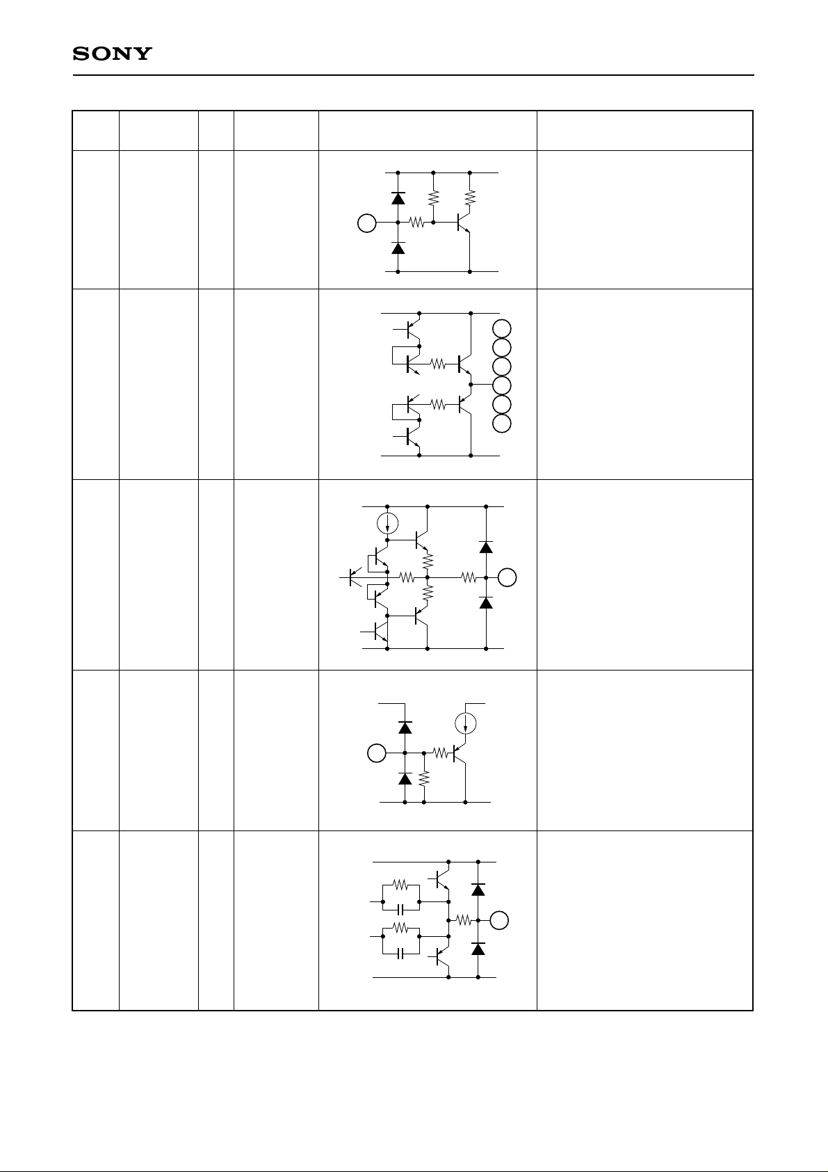
CXA7000R
Pin
No.
18
20
22
27
29
31
33
Symbol I/O
SH_OUT6
to
SH_OUT1
VCOM_OUT
Standard
voltage level
IDCFBOFF16
1.5 to 13.5V
O
5.0 to 8.0V
O
GND
Equivalent circuit Description
V
16
DD
145
24k
24k
Offset cancel function off.
Normally connect to GND to
use with the offset cancel
function on.
High (offset cancel function off)
when open.
GND
PVCC
18
300
300
GND
V
CC
80µ
20
22
27
29
31
Demultiplexed output of AC
inverse driven video signals.
Can be connected directly to
the LCD panel.
LCD panel common voltage
output.
Can be set in the range from
the SH_OUT center potential
Vsig.c to Vsig.c – 2V by
100k
500
500
145
33
VCOM_OFST.
VCOM_OFST
34
GND
VDD VCC
80µ
2k
100
145
36
GND
VCC
34
100k
0.2p
0 to 5.0VI
1.5 to 13.5VOSID_OUT36
100k
LCD panel common voltage
adjustment.
VCOM_OUT can be set in the
range from the SH_OUT center
potential Vsig.c to Vsig.c – 2V
by inputting 0 to 5V.
Precharge waveform output.
These pins cannot directly drive
the LCD panel, so input to the
LCD panel with an external
buffer.
GND
0.2p
– 4 –
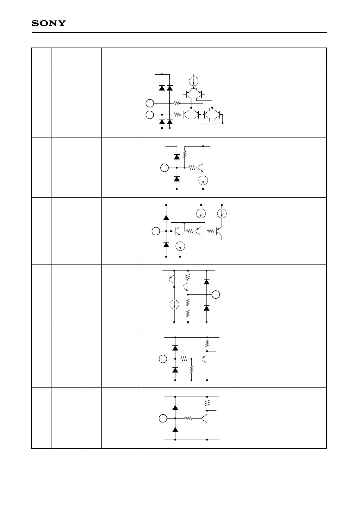
CXA7000R
Pin
No.
37
38
Symbol I/O
PRG_LV
SID_LV
Standard
voltage level
1.0 to 5.0V
I
High: ≥2.0V
IPRG39
Low: ≤0.8V
Equivalent circuit Description
VDD VCC
29µ
Precharge level setting.
Adjusts the SID_OUT and
37
50k
50k
38
SID_OUTX output potential.
PRG_LV is reflected when the
PRG input pin (Pin 60) is high,
and SID_LV is reflected when
PRG is low.
GND
V
DD
100k
39
GND
V
DD
10k
70µ 10µ
V
50µ
CC
Timing pulse input for switching
the Pin 36 output levels.
(See PRG_LV (Pin 37) and
SID_LV (Pin 38).)
Internal D/A converter reference
3.2VIVREF_I44
44
1k
33.3k
voltage input.
Normally connect directly to
VREF_O.
280µ
GND
High: ≥2.0V
Low: ≤0.8V
IF/H_CNT46
Open: Low
High: ≥2.0V
IDIRC47
Low: ≤0.8V
VDD
2k
Reference voltage output.
3.2VOVREF_O45
20µ
GND
VDD
46
20k
12.4k
192
200k
45
50k
Normally connect directly to
VREF_I, and connect to GND
through a 0.5 to 1.0µF capacitor.
SH_OUT output timing selection.
High: SH_OUT1 to SH_OUT3
and SH_OUT4 to SH_OUT6
are output at different timing.
Low: SH_OUT1 to SH_OUT6
are output at the same timing.
GND
VDD
50k
192
47
Scan direction setting.
High: output as a time series in
ascending order of output pin
symbol (in order from SH_OUT1
to SH_OUT6)
GND
Low: output in descending order
– 5 –
CXA7000R
Pin
No.
51
to
55
58
to
62
Symbol I/O
D_IN9 to
D_IN0
Standard
voltage level
High: ≥2.0V
Low: ≤0.8V
ISL_DAT48
Open: Low
High: ≥2.0V
ISTATUS50
Low: ≤0.8V
High: ≥2.0V
I
Low: ≤0.8V
Equivalent circuit Description
VDD
GND
V
DD
50
48
192
192
200k
200k
50k
50k
Digital input mode switch setting.
High: when using master/slave
mode two CXA7000R.
Low: when using normal mode
one CXA7000R.
Master/slave setting when using
two CXA7000R.
High: master IC. Offset cancel
level is output.
Low: slave IC. This pin is left
open (high) when using one
GND
VDD
to
to
GND
50k
192
5551
6258
CXA7000R.
Digital data input.
63
64
24, 25
17, 32
35
43
MCLK
MCLKX
PGND
PVCC
VCC15
VDD5
PECL
differential
(amplitude
0.4V or more
I
between
VDD to 2V)
or TTL input
GND
15.5V
15.5V
5VIPS42
5V
V
DD
63
64
GND
VDD
42
GND
1k
1k
70k
140k
60k 60k100µ
180k
140k8k
Dot clock input.
PECL differential input or TTL
input. For TTL input, input to
MCLK and connect MCLKX to
GND through a capacitor.
Test.
Normally connect to VDD.
30µ
Power GND.
Po wer VCC.
15V power supply.
5V power supply.
– 6 –
CXA7000R
Pin
No.
8, 9, 15,
23, 26,
40, 41,
56, 57
10, 19,
21, 28,
30
Symbol I/O
GND
NC
Standard
voltage level
1.7 to 3.2V
OTEST49
GND
2.5VISHTEST7
V
DD
7
GND
Equivalent circuit Description
GND.
NC.
These pins are not connected to
anything.
20k 20k
250k
192
20k
20k
Test.
Leave open.
250k
V
DD
1µ
10µ
2k
192
49
10µ
DAC output monitor test.
Normally connect to VDD.
GND
20µ
– 7 –
 Loading...