

Sony CXA3572R Datasheet
CXA3572R
Driver/Timing Generator for Color LCD Panels
Description
The CXA3572R is an IC designed to drive the color
LCD panel ACX306/312.
This IC greatly reduces the number of peripheral
circuits and parts by incorporating a RGB driver and
timing generator for video signals and a VCO onto a
single chip. This chip has a built-in serial interface
circuit and electronic attenuators which allow various
settings to be performed by microcomputer control,
etc.
Features
• Color LCD panel ACX306/312 driver
• Supports NTSC and PAL systems
• Supports Y/color difference and RGB inputs
• Supports OSD input
• Power saving function (clock stopped)
• Various setting control using a serial interface
circuit (asynchronous type)
• Electronic attenuators (D/A converter)
• VCO (no external oscillator circuit)
• LPF (fc variable)
• COMMON and PSIG output circuits
• Sharpness function
• 2-point γ correction circuit
• R, G, B signal delay time adjustment circuit
• Sync separation circuit
• D/A output pin (0 to 3V, 8 level output)
• Output polarity inversion circuit
• Supports AC drive for LCD panel during no signal
Applications
Compact LCD monitors, etc.
Absolute Maximum Ratings (Ta = 25°C)
• Supply voltage VCC1 5.5 V
• Analog input pin voltage
VINA1 (Pins 18, 19, 20, 22, 23, 24 and 25)
VINA2 (Pin 16) GND – 0.3 to VCC2 + 0.3 V
• Digital input pin voltage
VIND (Pins 34 and 35) VSS – 0.3 to +5.5 V
• Common input pin voltage
VINAD (Pins 31, 32 and 33)
• Operating temperature Topr –15 to +75 °C
• Storage temperature Tstg –55 to +150 °C
• Allowable power dissipation (Ta ≤ 25°C)
Operating Conditions
• Supply voltage VCC1 – GND1 2.7 to 3.6 V
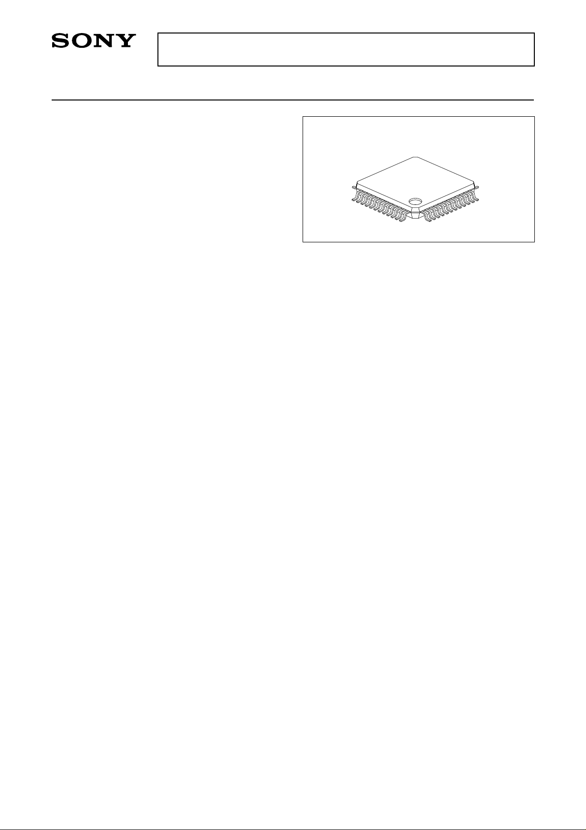
48 pin LQFP (Plastic)
VCC215 V
VDD 4.6 V
GND – 0.3 to VCC1 + 0.3 V
GND , VSS – 0.3 to +5.5 V
PD 600 mW
VCC2 – GND2 11.0 to 14.0 V
VDD – VSS 2.7 to 3.6 V
Sony reserves the right to change products and specifications without prior notice. This information does not convey any license by
any implication or otherwise under any patents or other right. Application circuits shown, if any, are typical examples illustrating the
operation of the devices. Sony cannot assume responsibility for any problems arising out of the use of these circuits.
– 1 –
E00Y05A11-PS

Block Diagram
CXA3572R
SYNC IN
DA OUT
REF
FILTER
RPD
GND1
SEN
SCK
SDAT
VD
XCLR
POF
B/B-Y
R/R-Y
G/Y
1
CC
V
+3V
OSD G
OSD R
OSD B
NC
SIG.C
PSIG DC DET
2
CC
PSIG OUT
V
+12V
131415161718192021222324
PICTURE Gain
ATT
25
ATT
ATT
26
27
LPF
LPF
TRAP
SW
28
29
DA
REF
LPF
DA
SUBCONTRAST
TRAP
SUB-
R, G, B
CONTRAST
CONTRAST
CONT R
SUB-
CONT B
PHASE
COMPARATOR
30
31
32
DAC
SERIAL I/F
33
IR
PICTURE
HUE
COLOR
COLOR
HUE
SYNC SEP
CLOCK
GENERATOR
RP
PICTURE f0
DL
MATRIX
DL
USERBRIGHT
USERBRIGHT
SYNC SEL
VCO ADJ
Fine
CK
GAMMA1
GAMMA2
VCO ADJ
Coarse
HD_
MODE
γ2
γ1
Analog block 3V
BLK
CSYNC
SUBBRIGHT
R-
XCLP
BRIGHT
S/H
BLIM
SH1
FRP
B-
BRIGHT
SH2
PSIGBRIGHT
PSIG-
BRIGHT
OSD
BLIM
COM
SH4
SH3
PSIG
PowerSW
XSTBY1
COM
Analog block 12V
XSTBY2
FRP
12
11
10
9
8
7
6
5
G OUT
G DC DET
R OUT
R DC DET
B OUT
B DC DET
COM
GND2
Digital block 3V
TEST
4
SERIAL I/F
34
35
PLL
COUNTER
TIMING GENERATOR
H. FILTER
VST
3
VCK
2
EN
1
36
+3V
0V
+3V
37 38 39 40 41 42 43 44 45 46 47 48
DD
V
HDO
VDO
RGT
SS
V
HCK1
HCK2
HST
DD
V
WIDE
DWN
– 2 –
0V
SS
V

Pin Description
CXA3572R
Pin
No.
EN
1
VCK
2
VST
3
TEST
4
GND2
5
COM
6
B DC DET
7
B OUT
8
R DC DET
9
R OUT
10
G DC DET
11
G OUT
12
VCC2
13
PSIG OUT
14
PSIG DC DET
15
SIG.C
16
Symbol
I/O
O
EN pulse output
O
V clock pulse output
O
V start pulse output
—
Test (Leave this pin open.)
—
Analog 12.0V GND
O
Common pad voltage output for LCD panel
O
B signal DC voltage feedback circuit capacitor connection
O
B signal output
O
R signal DC voltage feedback circuit capacitor connection
O
R signal output
O
G signal DC voltage feedback circuit capacitor connection
O
G signal output
—
Analog 12.0V power supply
O
PSIG output
O
PSIG signal DC voltage feedback circuit capacitor connection
I
R, G, B and PSIG output DC voltage adjustment
Description
Input pin for
open status
17
18
19
20
21
22
23
24
25
26
27
28
29
30
31
32
33
34
NC
OSD B
OSD R
OSD G
VCC1
G/Y
R/R-Y
B/B-Y
SYNC IN
DA OUT
REF
FILTER
RPD
GND1
SEN
SCK
SDAT
VD
—
I
OSD B input
I
OSD R input
I
OSD G input
—
Analog 3.0V power supply
I
G/Y signal input
I
R/R-Y signal input
I
B/B-Y signal input
I
Sync separation circuit input/sync signal input
O
DAC output
O
Level shifter circuit REF voltage output for LCD panel
O
Internal filter circuit f0 adjusting resistor connection
O
Phase comparator output
—
Analog 3.0V GND
I
Serial load input
I
Serial clock input
I
Serial data input
I
Vertical sync signal input
L
35
36
XCLR
POF
I
Power-on reset capacitor connection (timing output block)
LCD panel power supply on/off
O
(Leave this pin open when not using this function.)
– 3 –

CXA3572R
Pin
No.
37
38
39
40
41
42
43
44
45
46
47
48
Symbol
VDD
HDO
VDO
RGT
SS
V
HCK1
HCK2
HST
VDD
WIDE
DWN
VSS
I/O
—
Digital 3.0V power supply
O
HDO pulse output
O
VDO pulse output
O
Right/left inversion switching signal output
—
Digital 3.0V GND
O
H clock pulse 1 output
O
H clock pulse 2 output
O
H start pulse output
—
Digital 3.0V power supply
O
WIDE pulse output
O
Up/down inversion switching signal output
—
Digital 3.0V GND
Description
Input pin for
open status
– 4 –

Analog Block Pin Description
CXA3572R
Pin
No.
Symbol
Pin
voltage
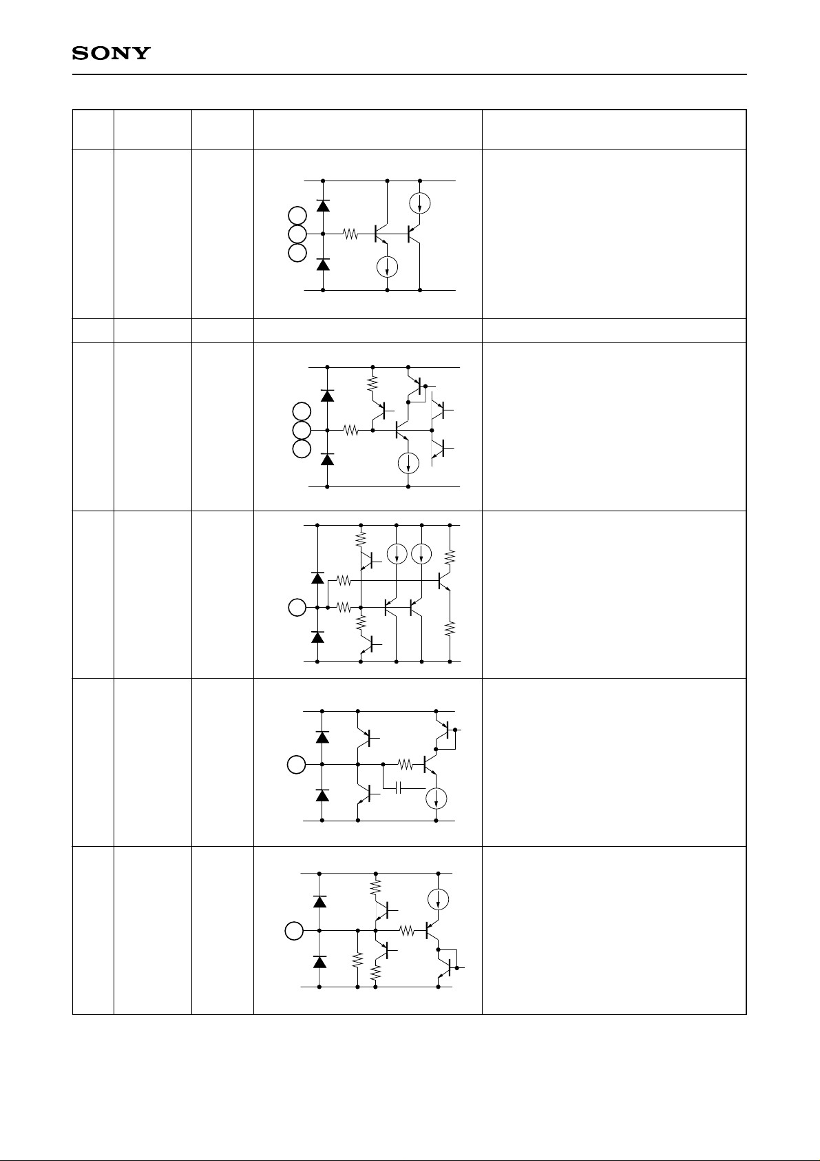
5 GND2 —
6 COM —
7
B DC DET
9
R DC DET
11
G DC DET
15
PSIG DC DET
3.0V
Vcc2
GND2
Vcc2
GND2
Equivalent circuit Description
Analog 12.0V GND.
11
15
4K
10k
125k
5k
5k
6
100k
7
9
COMMON voltage output.
The output voltage is controlled by serial
communication.
Smoothing capacitor connection for the
feedback circuit of R, G, B and PSIG
output signal DC level control.
Connect a low-leakage capacitor.
8
B OUT
10
12
14
R OUT
G OUT
PSIG OUT
—
16 SIG.C VCC/2
Vcc2
10
12
14
GND2
Vcc2
GND2
8
100k
10
10
500
5k
R, G, B and PSIG signal outputs.
The DC level is controlled to match the
SIG.C pin voltage.
Low output in power saving mode.
Analog 12.0V power supply.13 VCC2 12.0V
R, G, B and PSIG output DC voltage
200k
setting.
Connect a 0.01µF capacitor between
16
200k
10p
this pin and GND1.
When using a SIG.C of other than
Vcc2/2, input the SIG.C voltage from an
external source.
No connection.17 NC —
– 5 –
CXA3572R
Pin
No.
18
19
20
22
23
24
Symbol Equivalent circuit Description
OSD B
OSD R
OSD G
Pin
voltage
Vth1 =
VCC1 ×
1/3
Vth2 =
VCC1 ×
2/3
Vcc1
18
19
20
GND1
20k
OSD pulse inputs.
When one of these input pins exceeds
the Vth1 level, all of the outputs go to
black limiter level; when an input pin
exceeds the Vth2 level, only the
corresponding output goes to white
limiter level.
Connect these pins to GND when not
used.
Analog 3.0V power supply.21 VCC13.0V
G/Y
R/R-Y
B/B-Y
G/Y:
1.8V
R/R-Y,
B/B-Y,
RGB:
1.8V
Y/color
difference:
Vcc1
22
23
24
GND1
1k
In Y/color difference input mode, input
the Y signal to Pin 22, the R-Y signal to
Pin 23 and the B-Y signal to Pin 24.
In RGB input mode, input the G signal
to Pin 22, the R signal to Pin 23 and the
B signal to Pin 24.
Pedestal clamp these pins with external
coupling capacitors.
2.0V
25 SYNC IN 0.9V
26 DA OUT —
27 REF VCC1/2
Vcc1
25
GND1
Vcc1
26
GND1
Vcc1
27
10k
1k
100k
80k
15p
25k
Sync separation circuit input, or composite
sync/horizontal sync signal input.
During input to the sync separation
circuit, input via a capacitor.
DA output.
Outputs the serial data converted to DC
voltage. The current driving capacity is
±1.0mA (max.).
REF output.
The current driving capacity (sink) is
1.6mA (max.).
GND1
– 6 –

CXA3572R
Pin
No.
Symbol Equivalent circuit Description
Pin
voltage
28 FILTER 1.2V
RPD
Vcc1
GND1
Vcc1
29
GND1
28
500
1k 100k
Connect a resistor between this pin and
GND1 to control the internal LPF and
trap frequencies.
Connect a 43kΩ resistor (tolerance ±2%,
temperature characteristics ±200ppm or
less).
This pin is easily affected by external
noise, so make the connection between
the pin and external resistor, and
between the GND side of the external
resistor and the GND1 pin as close as
possible.
Phase comparator output.29 1.8V
31
32
33
SEN
SCK
SDAT
—
Vcc1
31
32
33
GND1
Vss
Analog 3.0V GND.30 —GND1
1
∗
20k
Serial clock, serial load and serial data
inputs for serial communication.
– 7 –
Digital Block Pin Description
CXA3572R
Pin
No.
1
2
3
36
38
39
40
42
43
44
46
47
35
31
32
33
Symbol Equivalent circuit Description
Pin
voltage
EN
VCK
VST
POF
HDO
VDO
RGT
—
1
36
40
44
2
38
42
46
3
39
43
47
Digital block outputs.
HCK1
HCK2
Vss
HST
WIDE
DWN
XCLR
SEN
SCK
SDAT
—
353132
33
Vss
Digital block system reset, and serial
clock, serial load and serial data inputs
for serial communication.
37
VDD —
45
41
VSS —
48
4 TEST —
34
Vertical sync signal input.34 VD —
Vss
Digital 3.0V power supply.
Digital 3.0V GND.
Test.
Leave this pin open.
– 8 –

CXA3572R
Setting Conditions for Measuring Electrical Characteristics
Use the Electrical Characteristics Measurement Circuit on page 21 when measuring electr ical characteristics.
For measurement, the digital block must be initialized and power saving must be canceled by performing
Settings 1, 2 and 3 below. In addition, the serial data must be set to the initial settings shown in the table below.
Setting 1. System reset
After turning on the power, activate the TG block system reset by setting XCLR (Pin 35) Low.
The serial bus is set to the default values.
V
DD
XCLR (Pin 35)
T
R
TR > 10µs
Setting 2. Horizontal AFC adjustment
In the condition without sync input, adjust so that the HDO pulse output frequency is
NTSC: 15.734 ± 0.1kHz and PAL: 15.625 ± 0.1kHz.
Setting 3. Canceling power saving mode
The power-on default is power saving mode, so clear (set all “1”) serial data PS0 and SYNC GEN.
System reset
– 9 –

Serial data initial settings
CXA3572R
MSB
A7
0
0
0
0
0
0
0
0
0
0
0
0
0
0
0
0
0
A6
0
0
0
0
0
0
0
0
0
0
0
0
0
0
0
0
0
A5
0
0
0
0
0
0
0
0
0
0
0
0
0
0
0
0
0
A4
0
0
0
0
0
0
0
0
0
0
0
0
0
0
0
0
1
A3
0
0
0
0
0
0
0
0
1
1
1
1
1
1
1
1
0
A2
0
0
0
0
1
1
1
1
0
0
0
0
1
1
1
1
0
LSBADDRESS MSB LSBDA TA
A1
0
0
1
1
0
0
1
1
0
0
1
1
0
0
1
1
0
A0
D7 D6 D5 D4 D3 D2 D1 D0
0
1
0
1
0
1
0
1
PSIGSW
0
1
0
1
0
0
0
0
0
0
(0)
0
0
0
USER-BRIGHT (10000000/LSB)
SUB-BRIGHT R (1000000/LSB)
SUB-BRIGHT B (1000000/LSB)
CONTRAST (10000000/LSB)
SUB-CONTRAST R (1000000/LSB)
SUB-CONTRAST B (1000000/LSB)
PSIG-BRIGHT (1000000/LSB)
0
1
0
1
0
0
LPFSW
(0)
0
0
BLACK-LIMITER (100000/LSB)
PICTURE-GAIN (00000/LSB)
0
VCO Coarse (000/LSB)
γ-1 (0000000/LSB)
γ-2 (0000000/LSB)
COM-DC (1000000/LSB)
COLOR (1000000/LSB)
HUE (1000000/LSB)
VCO Fine (10000000/LSB)
PICTURE-F0 (000/LSB)
TRAP
(0)
DA (000/LSB)LPF (000/LSB)
INPUT
SEL (0)
SYNC
SEL (1)
MODE
(0)
0
1
0
0
0
0
0
0
0
1
0
0
0
0
0
1
0
1
0
0
0
0
1
0
0
1
0
0
0
0
1
1
0
1
0
0
0
1
0
0
0
1
0
0
0
1
0
1
0
1
0
0
0
1
1
0
0
SLSYP
SYST
(1)
(0)
0
SLEXVD
(1)
SLFL
(0)
SLMBK
(0)
S/H POSITION (000/LSB)
SB POSITION (100/LSB)
0
TEST2
(1)
SLDWN
(0)
SLFR
(0)
PONF
(1)
SLRGT
(0)
SL4096
(0)
TEST4 (00000000/LSB)
TEST1
(0)
SLCLP1
(0)
H POSITION (100000/LSB)
HDO POSITION (00000/LSB)
V POSITION (01000/LSB)
SLPOF
(0)
TEST3
(0, 0)
SLCLP0
(0)
SYNC
GEN (1)
SLWD
(0)
SLVDO
(0)
PS0
(1)
SLNTPL
(0)
SLHDO
(0)
Note: If there is the possibility that data may be set at other than the above-noted addresses, set these data to “0”.
– 10 –
Electrical Characteristics — DC Characteristics
Analog Block
(Ta = 25°C, VCC1 = VDD = 3.0V, VCC2 = 12.0V, see page 10 for the DAC)
CXA3572R
Item
Current consumption 1
(Y/color difference input)
Current consumption 2
(Y/color difference input)
Current consumption 1
(RGB input)
Current consumption 2
(RGB input)
Current consumption 1
(PS0 = 0)
Current consumption 2
(PS0 = 0)
Current consumption 1
(SYNC GEN = 0)
Current consumption 2
(SYNC GEN = 0)
B DC DET pin voltage
R DC DET pin voltage
G DC DET pin voltage
PSIG DC DET pin voltage
SIG.C pin voltage
G/Y pin voltage
Symbol Measurement conditions
I1
I2
IRGB1
IRGB2
IPS01
IPS02
ISG1
ISG2
Measure the inflow current
to Pin 21.
Measure the inflow current
to Pin 13.
Measure the inflow current
to Pin 21.
Measure the inflow current
to Pin 13.
Measure the inflow current
to Pin 21.
Measure the inflow current
to Pin 13.
Measure the inflow current
to Pin 21.
Measure the inflow current
to Pin 13.
V7
V9
V11
V15
V16
V22
Min. Typ. Max. Unit
16
1.0
12
1.0
34
3.4
28
3.4
50
10
42
10
mA
—
—
—
—
7
0.3
14
0.3
11
1.0
27
1.0
3.0
3.0
3.0
3.0
6.0
1.8
R/R-Y pin voltage 1
R/R-Y pin voltage 2
B/B-Y pin voltage 1
B/B-Y pin voltage 2
SYNC IN pin voltage
REF pin voltage
(power saving mode)
FILTER pin voltage
OSD R, G, B input voltage
SIG. C input voltage
V23
V23
V24
V24
V25
V27
V28
VSIG.C
During Y/color difference
input
During RGB input
During Y/color difference
input
During RGB input
During no input
– 11 –
GND
5.0
2.0
1.8
2.0
1.8
1.1
0.2
1.2
V
VCC1
6.5
CXA3572R
Item
Y/Color difference mode
Y, R-Y, B-Y signal input
level 1
Symbol Measurement conditions Min. Typ. Max. Unit
1
∗
Y
SYNC
(Y on SYNC)
R-Y
B-Y
1
∗
Y
Y/Color difference mode
Y, R-Y, B-Y signal input
level 2
SYNC
(Y on SYNC)
R-Y
B-Y
RGB mode
R, G, B signal input
level 1
RGB mode
R, G, B signal input
level 2
1
∗
Y signal level (SYNC level is not included.)
2
∗
SYNC level of Y (G) on SYNC signal.
R, G, B
SYNC
(G on SYNC)
R, G, B
SYNC
(G on SYNC)
∗
∗
2
INPUT SEL = 0
∗
0.35
0.15
0.4
0.2
(–6dB Attenuate OFF)
0.245
0.311
0.7
INPUT SEL = 1
2
∗
(–6dB Attenuate ON)
0.3
0.490
Vp-p
0.622
1
INPUT SEL = 0
(–6dB Attenuate OFF)
2
∗
1
INPUT SEL = 1
(–6dB Attenuate ON)
2
∗
0.35
0.15
0.5
0.2
0.7
0.3
– 12 –
 Loading...