

Sony CXA3555N Datasheet

All Band Tuner IC with On-chip PLL
Description
The CXA3555N is a monolithic TV tuner IC which
integrates local oscillator and mixer circuits for VHF
band, local oscillator and mixer circuits for UHF
band, an IF amplifier and a tuning PLL onto a single
chip, enabling further miniatur ization of the tuner.
Features
• Low power consumption (5V, 63mA typ.)
• Low noise figure, low distortion characteristics
• High gain/low gain selectable
• Supports IF double-tuned/adjacent channel trap
• Balanced oscillator circuits (3 sets) with excellent
oscillation stability
• On-chip PLL supports I2C bus
• On-chip high voltage drive transistor for charge
pump
• Frequency step selectable from 31.25, 50 or
62.5kHz (when using a 4MHz crystal)
• Low-phase noise synthesizer
• On-chip 4-output band switch (output voltage: 5V,
current capacity: 5mA)
• 30-pin SSOP small package
CXA3555N
30 pin SSOP (Plastic)
Absolute Maximum Ratings
• Supply voltage VCC –0.3 to +5.5 V
• Operating temperature Topr –25 to +75 °C
• Storage temperature Tstg –55 to +150 °C
• Allowable power dissipation
PD 580 mW
Operating Conditions
Supply voltage VCC 4.75 to 5.30 V
Applications
• TV tuners
• VCR tuners
• CATV tuners
Structure
Bipolar silicon monolithic IC
Note: This IC has pins whose electrostatic discharge strength is weak as the operating frequency is high
and the high-frequency process is used for this IC. Take care of handling the IC.
Sony reserves the right to change products and specifications without prior notice. This information does not convey any license by
any implication or otherwise under any patents or other right. Application circuits shown, if any, are typical examples illustrating the
operation of the devices. Sony cannot assume responsibility for any problems arising out of the use of these circuits.
– 1 –
E01326-PS
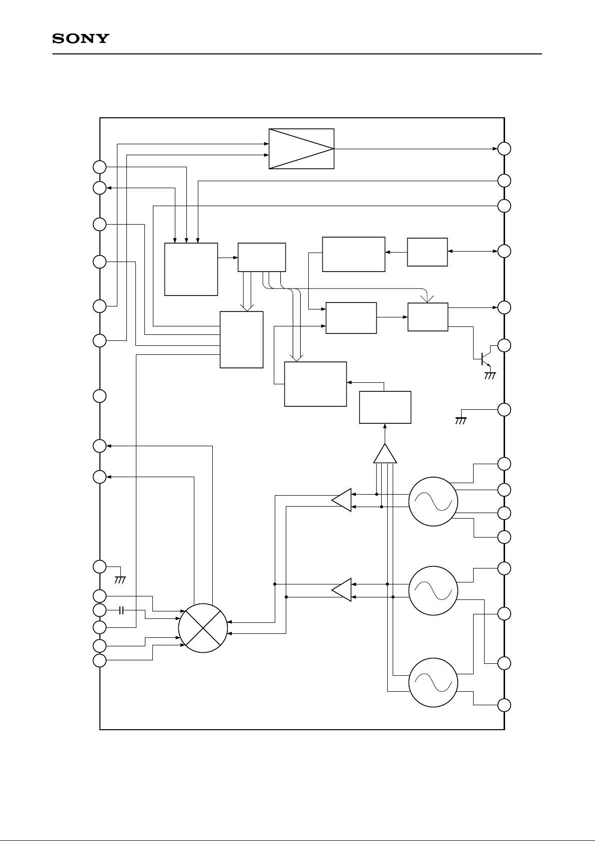
Block Diagram and Pin Configuration
CXA3555N
SCL
SDA
BS1
BS2
IFIN1
IFIN2
Vcc
IF AMP
1
2
3
4
5
6
7
2
C BUS
I
Interface
Shift
Register
Band SW
Driver
Programable
Divider
14/15 bit
Divider
1/128, 160, 256
Phase
Detector
Prescaler
1/2
REF
OSC
Charge
Pump
30
29
28
27
26
25
24
IFOUT
ADSW
BS3
REF
OSC
CPO
VT
GND2
MIXOUT1
MIXOUT2
GND1
VHFIN
BYP
BS4
UHFIN1
UHFIN2
10
11
12
13
14
15
8
23
UOSCB2
9
22
UOSCE2
21
UOSCE1
UHFOSC
VHOSC
UHF/VHF
MIX
VLOSC
20
19
18
17
16
UOSCB1
VHOSC2
VLOSC2
VHOSC1
VLOSC1
– 2 –
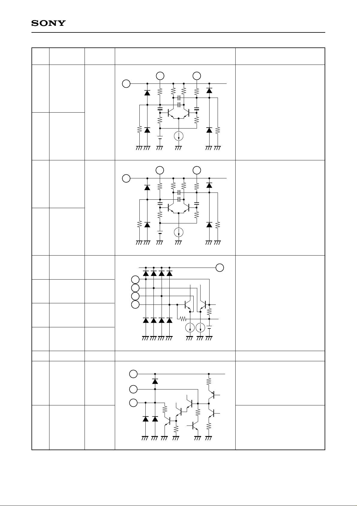
Pin Description
CXA3555N
Pin
No.
1
2
3
4
5
6
7
8
9
10
11
12
13
14
15
16
Symbol
SCL
SDA
BS1
BS2
IFIN1
IFIN2
Vcc
MIXOUT1
MIXOUT2
GND1
VHFIN
BYP
BS4
UHFIN1
UHFIN2
VLOSC1
Description
SCL input
SDA I/O
Band switch output 1
Band switch output 2
IF amplifier input
IF amplifier input
Power supply
MIX output (open collector)
MIX output (open collector)
Analog circuit GND
VHF input
VHF input GND and gain switching (low: GND, high: open)
Band switch output 4
UHF input
UHF input
VHF Low-band oscillator
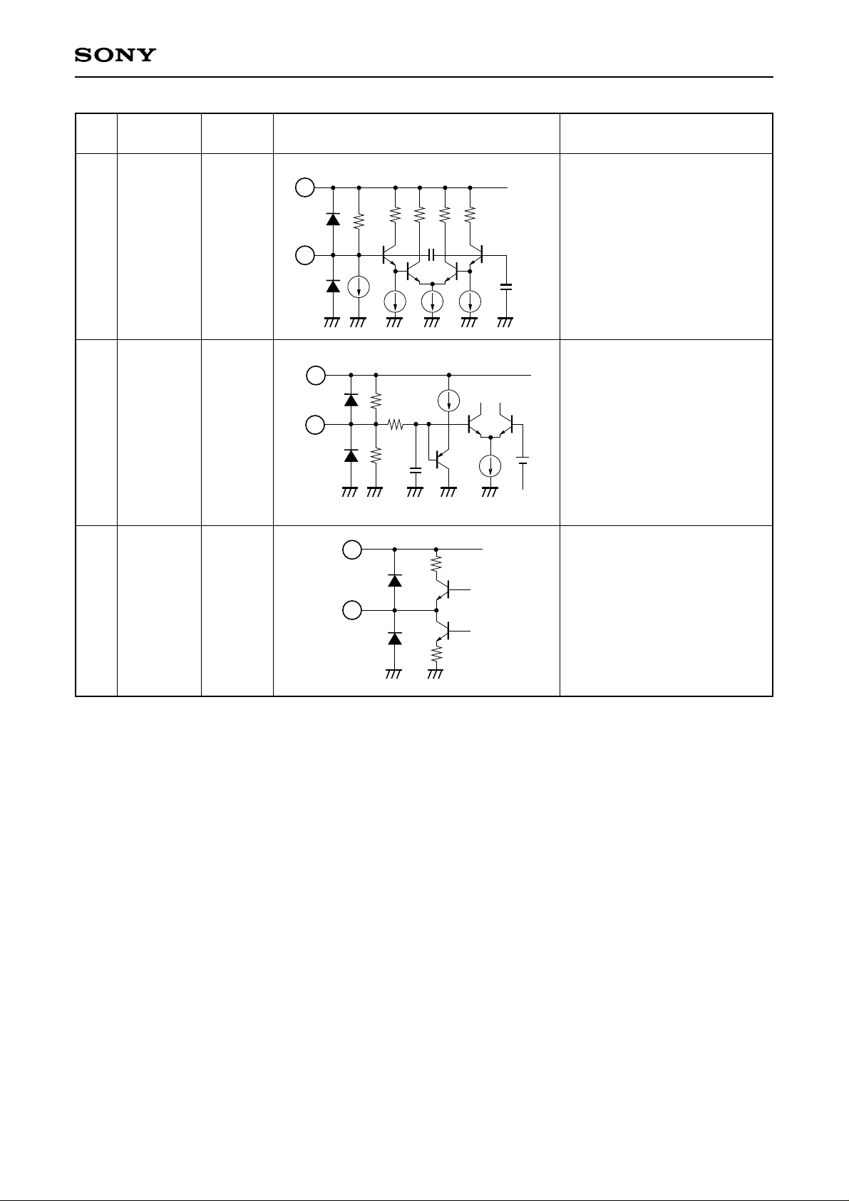
17
18
19
20
21
22
23
24
25
26
27
28
29
30
VHOSC1
VLOSC2
VHOSC2
UOSCB1
UOSCE1
UOSCE2
UOSCB2
GND2
VT
CPO
REFOSC
BS3
ADSW
IFOUT
VHF High-band oscillator
VHF Low-band oscillator
VHF High-band oscillator
UHF oscillator (base pin)
UHF oscillator (emitter pin)
UHF oscillator (emitter pin)
UHF oscillator (base pin)
PLL circuit GND
Tuning voltage output (open collector)
Charge pump output (loop filter connection)
Crystal connection for PLL reference oscillator
Band switch output 3
Address selection (I2C bus)
IF amplifier output
– 3 –
Pin Description
CXA3555N
Pin
No.
Symbol
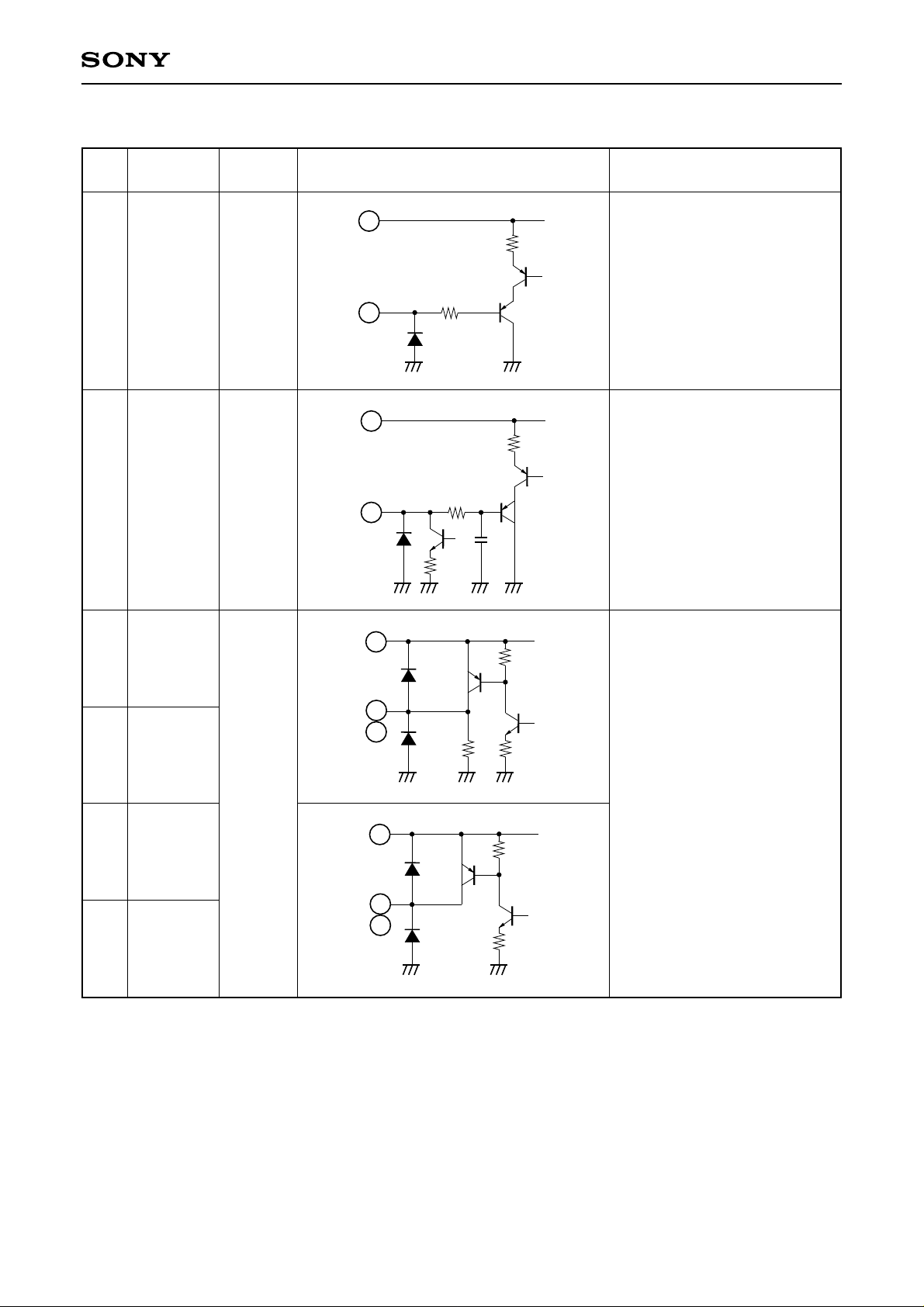
1 SCL — Clock input
2SDA — Data input
Pin voltage
[V]
Equivalent circuit Description
7
40k
1
7
40k
2
5p
3 BS1
4 BS2
13 BS4
28 BS3
High: 4.9
Low: 0.0
7
3
4
13
28
70k
Band switch outputs.
This pin corresponding to the
7
selected band goes High.
– 4 –
CXA3555N
Pin
No.
5 IFIN1
Symbol
Pin voltage
[V]
Equivalent circuit Description
7
5
1.6k
6
IF inputs.
2.0
These pins must be connected
to the mixer outputs via
coupling capacitance.
6 IFIN2
7VCC — Power supply.
8
9
8 MIXOUT1
Mixer outputs.
These pins output the signal in
—
open collector format, and they
must be connected to the
9 MIXOUT2
power supply via a load.
10 GND1 — Analog circuit GND.
11 VHFIN
2.4 during
VHF reception
0.0 during
UHF reception
7
11
3k 3k
15p
150k
57k
VHF input.
The input format is unbalanced
input.
VHF input GND and gain
switching.
12 BYP
VCC
(when open)
12
GND: low gain
Open: high gain
(However, when control byte
GC is "0")
7
14 UHFIN1
15 UHFIN2
0.0 during
VHF reception
2.3 during
UHF reception
14
15
3k 3k
UHF inputs.
Input a balanced signal to
Pins 14 and 15, or ground
either of Pin 14 or 15 with a
capacitor and input the signal
to the other pin.
– 5 –
CXA3555N
Pin
No.
Symbol
16 VLOSC1
18 VLOSC2
17 VHOSC1
19 VHOSC2
Pin voltage
[V]
0.0
0.0
Equivalent circuit Description
16 18
7
3333
External resonance circuit
connection for VL oscillator.
50k
17 19
7
2020
50k
External resonance circuit
connection for VH oscillator.
50k
50k
2.4 during
20 UOSCB1
21 UOSCE1
22 UOSCE2
23 UOSCB2
VHF reception
2.2 during
UHF reception
2.0 during
VHF reception
1.5 during
UHF reception
2.0 during
VHF reception
1.5 during
UHF reception
2.4 during
VHF reception
2.2 during
UHF reception
23
22
21
20
3k
3k
7
External resonance circuit
connection for UHF oscillator.
24 GND2 — PLL circuit GND.
7
25 VT —
26
Varicap drive voltage output.
This pin outputs the signal in
open collector format, and it
must be connected to the
tuning power supply via a load.
25
70
26 CPO 2.0
Charge pump output.
Connects the loop filter.
– 6 –
CXA3555N
Pin
No.
Symbol
Pin voltage
[V]
27 REFOSC 4.4
29 ADSW
1.25
(when open)
27
Equivalent circuit Description
7
30k
25p
Crystal connection for
reference oscillator.
38p
7
150k
29
Address selection.
Controls address bits 1 and 2.
50k
5p
7
30 IFOUT 2.8 IF output.
30
– 7 –
Electrical Characteristics (See the Electrical Characteristics Measurement Circuit.)
Circuit Current
(Vcc = 5V, IFVCC = 5V, Ta = 25°C)
CXA3555N
Item Symbol
Iccv
Circuit current
Iccu
OSC/MIX/IF Amplifier Block
Item Symbol
CG1
CG2
CG3
CG4
1
Conversion gain
∗
CG5
CG6
CG7
CG8
NF1
NF2
NF3
Noise figure
∗1, ∗
NF4
2
NF5
NF6
NF7
NF8
Measurement conditions
VCC current
Band switch output open during VHF operation
VCC current
Band switch output open during UHF operation
Measurement conditions
VHF operation fRF = 55MHz High gain mode
VHF operation fRF = 360MHz High gain mode
UHF operation fRF = 360MHz High gain mode
UHF operation fRF = 800MHz High gain mode
VHF operation fRF = 55MHz Low gain mode
VHF operation fRF = 360MHz Low gain mode
UHF operation fRF = 360MHz Low gain mode
UHF operation fRF = 800MHz Low gain mode
Min. Typ.
35
35
56
56
Min. Typ.
19.0
19.5
23.0
23.0
17.0
17.5
21.0
21.0
22.0
22.5
26.0
26.0
20.0
20.5
24.0
24.0
12
12
10
11
13
13
11
12
Max. Unit
78
78
mA
mA
Max. Unit
25.0
25.5
29.0
29.0
23.0
23.5
27.0
27.0
15
15
13
14
16
16
14
15
dB
dB
dB
dB
dB
dB
dB
dB
dB
dB
dB
dB
dB
dB
dB
dB
1% cross
modulation 1
∗1, ∗
Maximum output power
3
CM1
CM2
CM3
CM4
CM5
CM6
CM7
CM8
Pomax
VHF operation fD = 55MHz
fUD = ±12MHz (30% AM) High gain mode
VHF operation fD = 360MHz
fUD = ±12MHz (30% AM) High gain mode
UHF operation fD = 360MHz
fUD = ±12MHz (30% AM) High gain mode
UHF operation fD = 800MHz
fUD = ±12MHz (30% AM) High gain mode
VHF operation fD = 55MHz
fUD = ±12MHz (30% AM) Low gain mode
VHF operation fD = 360MHz
fUD = ±12MHz (30% AM) Low gain mode
UHF operation fD = 360MHz
fUD = ±12 MHz (30% AM) Low gain mode
UHF operation fD = 800MHz
fUD = ±12 MHz (30% AM) Low gain mode
50Ω load, saturation output
– 8 –
99
99
97
94
100
100
98
94
8
103
103
101
98
104
104
102
98
11
dBµ
dBµ
dBµ
dBµ
dBµ
dBµ
dBµ
dBµ
dBm
CXA3555N
Item Symbol
Switch ON drift
(PLL not
4
operating)
∗
Supply voltage drift
(PLL not
4
operating)
∗
Oscillator phase
noise
∆fsw1
∆fsw2
∆fsw3
∆fsw4
∆fst1
∆fst2
∆fst3
∆fst4
C/N1
C/N2
Measurement conditions
VHF operation fOSC = 100MHz
∆f from 3s to 3min after switch ON
VHF operation fOSC = 405MHz
∆f from 3s to 3min after switch ON
UHF operation fOSC = 405MHz
∆f from 3s to 3min after switch ON
UHF operation fOSC = 845MHz
∆f from 3s to 3min after switch ON
VHF operation fOSC = 100MHz
∆f when VCC 5V changes ±5%
VHF operation fOSC = 405MHz
∆f when VCC 5V changes ±5%
UHF operation fOSC = 405MHz
∆f when VCC 5V changes ±5%
UHF operation fOSC = 845MHz
∆f when VCC 5V changes ±5%
VHF operation 10kHz offset CP = 1
Phase comparison frequency = 31.25kHz
UHF operation 10kHz offset CP = 1
Phase comparison frequency = 31.25kHz
Min. Typ.
86
80
Max. Unit
±300
±600
±350
±400
±100
±450
±100
±100
kHz
kHz
kHz
kHz
kHz
kHz
kHz
kHz
dBc/Hz
dBc/Hz
1
∗
Value measured with untuned input.
2
∗
NF meter direct-reading value (DSB measurement).
3
∗
Value with a desired reception signal input level of –30dBm, an interference signal of 100kHz/30% AM,
and an interference signal level where S/I = 46dB measured with a spectrum analyzer.
4
∗
Value when the PLL is not operating.
– 9 –
 Loading...