


CXA3541N
2-channel Read/Write Amplifier for GMR-Ind Head Hard Disk Drive
Description
The CXA3541N is a read/write amplifier for GMR-Ind
(Giant Magneto Resistive-Inductive) heads used in
hard disk drives, and is capable of supporting up to
two channels.
Features
• +5V and –3V power supply
• Current bias voltage sense type
• Low power 180mW at read
• Differential read amplifier gain; ×100/135 (RMR = 50Ω)
• Input noise of 0.77nV/√ Hz (typ.), RMR = 50Ω,
IB = 5.9mA
• Recovery time write to read; 300ns (typ.)
• Write data is triggered by differential P-ECL signal
• Servo bank write
• Write unsafe detection circuit
• Serial port
Head selection
MR bias
Write current
Applications
Hard disk drives with GMR-Ind heads
Structure
Bipolar silicon monolithic IC
Absolute Maximum Ratings (Ta = 25°C)
• Supply voltage VCC –0.3 to +5.8 V
• Supply voltage VEE –3.7 to +0.3 V
• Digital input voltage Vdi –0.3 to VCC + 0.3 V
• Operating temperature Topr 0 to +70 °C
• Storage temperature Tstg –55 to +150 °C
• Allowable power dissipation
PD 800 mW
(on board)
Operating Conditions
• Supply voltage VCC 4.4 to 5.5 V
VEE –3.5 to –2.6 V
• MR bias voltage VMR –300 to +300 mV
• Bias current IB 3 to 8 mA
• Write current IW 19.5 to 49.5 mA
– 1 –
E00205-PS
Sony reserves the right to change products and specifications without prior notice. This information does not convey any license by
any implication or otherwise under any patents or other right. Application circuits shown, if any, are typical examples illustrating the
operation of the devices. Sony cannot assume responsibility for any problems arising out of the use of these circuits.
24 pin SSOP (Plastic)
– 2 –
CXA3541N
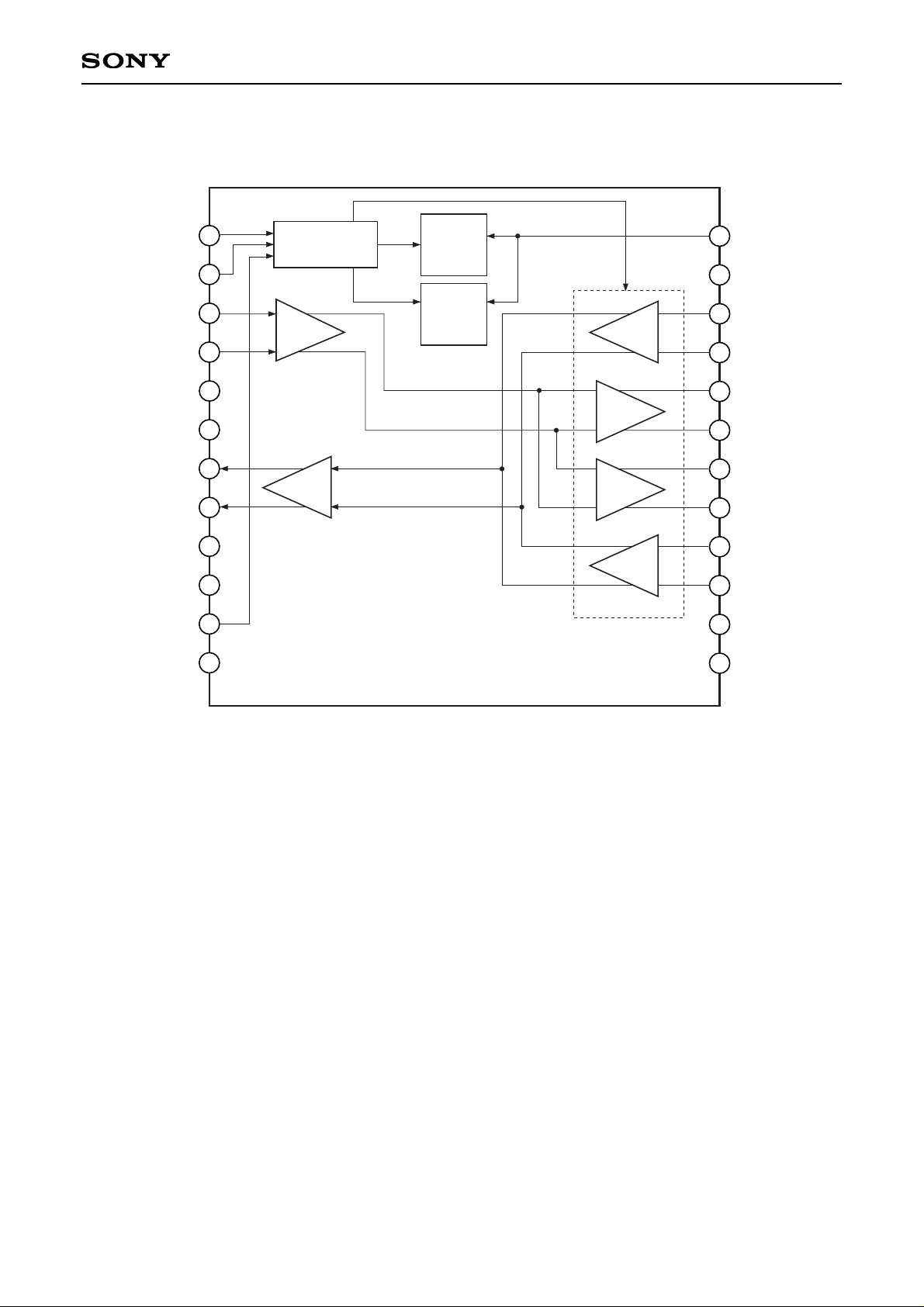
Block Diagram and Pin Configuration
RDX
FLT/SE/BHV
R/XW
SDEN
V
EE
RDY
GND
SCLK
SDATA
5
WDY
WDX
V
CC
R0Y
R0X
W0Y
W0X
W1Y
W1X
R1X
R1Y
DRIVER
DRIVER
AMP
15
NC
14
CAP
13
16
17
18
19
20
21
22
NC
23
RS
24
AMP
AMP
Bias
Current
Source
Write
Current
Source
Serial Interface
WD BUF
12
11
10
9
8
7
6
2
1
3
4
– 3 –
CXA3541N
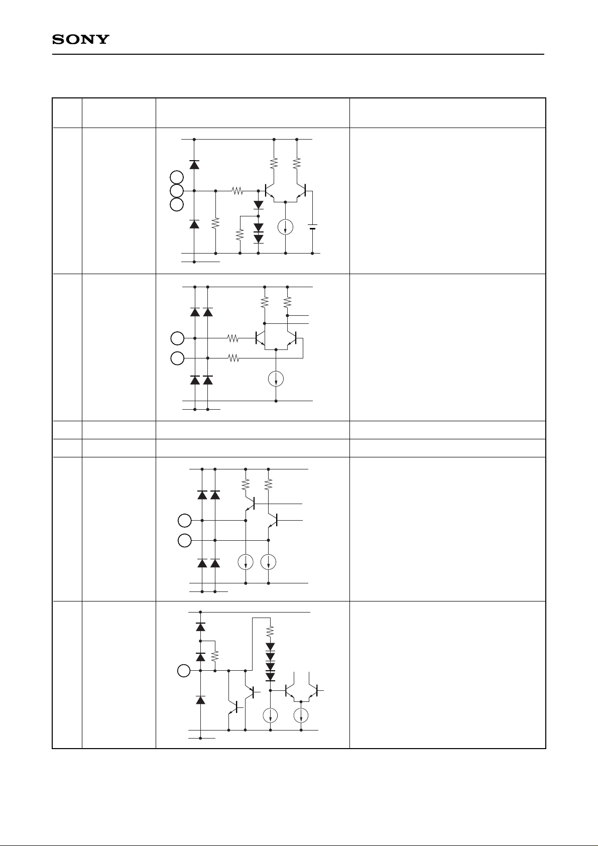
Pin Description
Pin
No.
Symbol Equivalent circuit Description
5
3
4
VCC
WDX
WDY
5V power supply.
Differential P-ECL write data input.
3
4
V
CC
VEE
100
100
GND
1
2
11
SCLK
SDATA
SDEN
Serial control signal input.
2
11
1
VCC
VEE
7.5k
14k
GND
2Vf
7
8
RDY
RDX
Read amplifier output with coupling
capacitors.
High impedance in the write mode.
7
8
V
CC
VEE
100
1.8mA
GND
6 GND
Ground.
9
FLT/SE/BHV
Head unsafe detection output.
Servo bank write enable input.
Buffered head voltage output.
9
V
CC
VEE
GND
– 4 –
CXA3541N
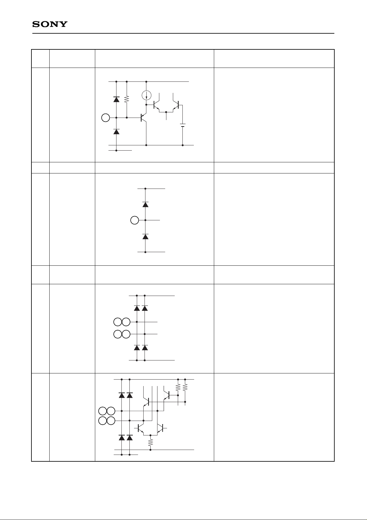
Pin
No.
Symbol Equivalent circuit Description
10
R/XW
Read/write control signal input.
Read when high, write when low.
10
VCC
VEE
GND
3Vf
13
CAP
Connect an external capacitor of read
amplifier between this pin and VEE.
13
V
CC
VEE
12
VEE
–3V power supply.
14
23
NC Non connection.
16
15
21
22
R0X
R0Y
R1X
R1Y
MR heads for read.
Two channels are provided.
21
22
16
15
V
CC
VEE
18
17
19
20
W0X
W0Y
W1X
W1Y
Inductive heads for write.
Two channels are provided.
19
20
18
17
V
CC
VEE
GND
– 5 –
CXA3541N
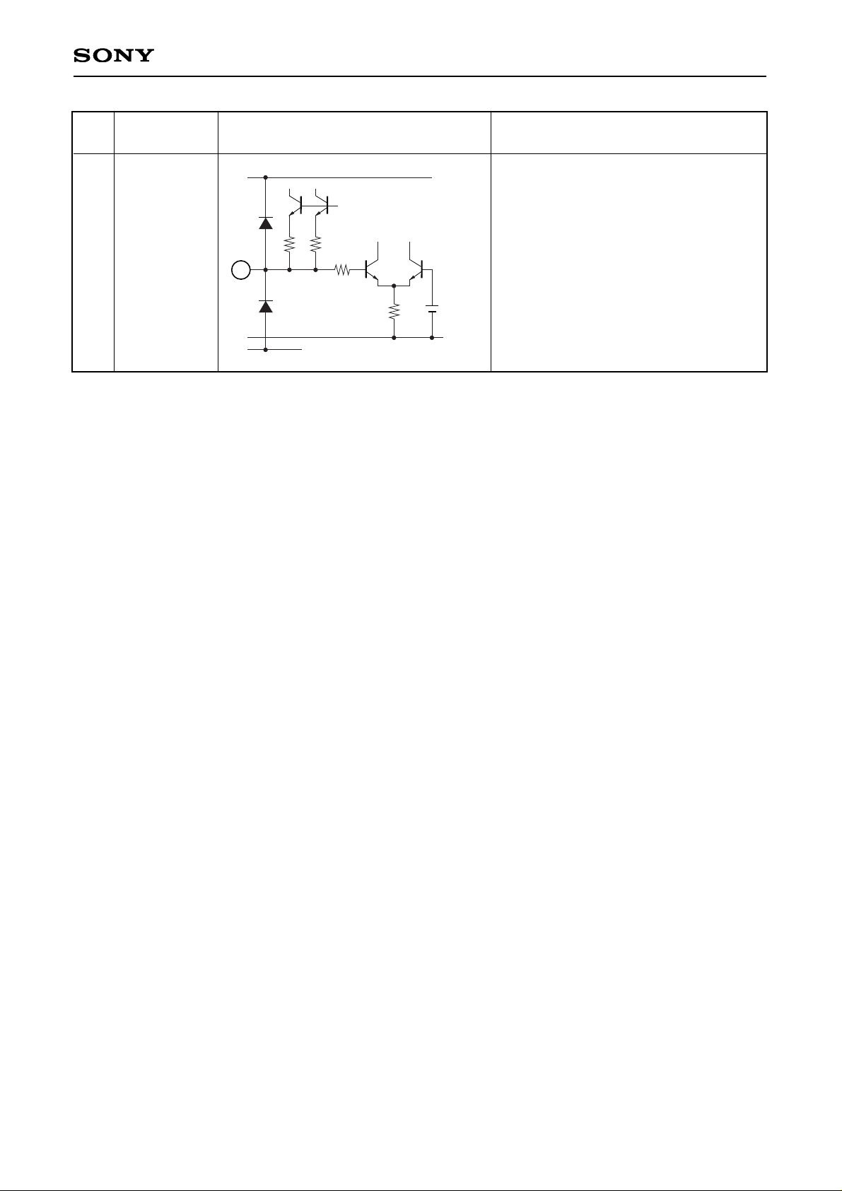
Pin
No.
Symbol Equivalent circuit Description
24 RS
Bias current setting register is connected
between this pin and GND.
24
V
CC
VEE
250
GND
VBGR
= 1.3V
– 6 –
CXA3541N
– 6 –
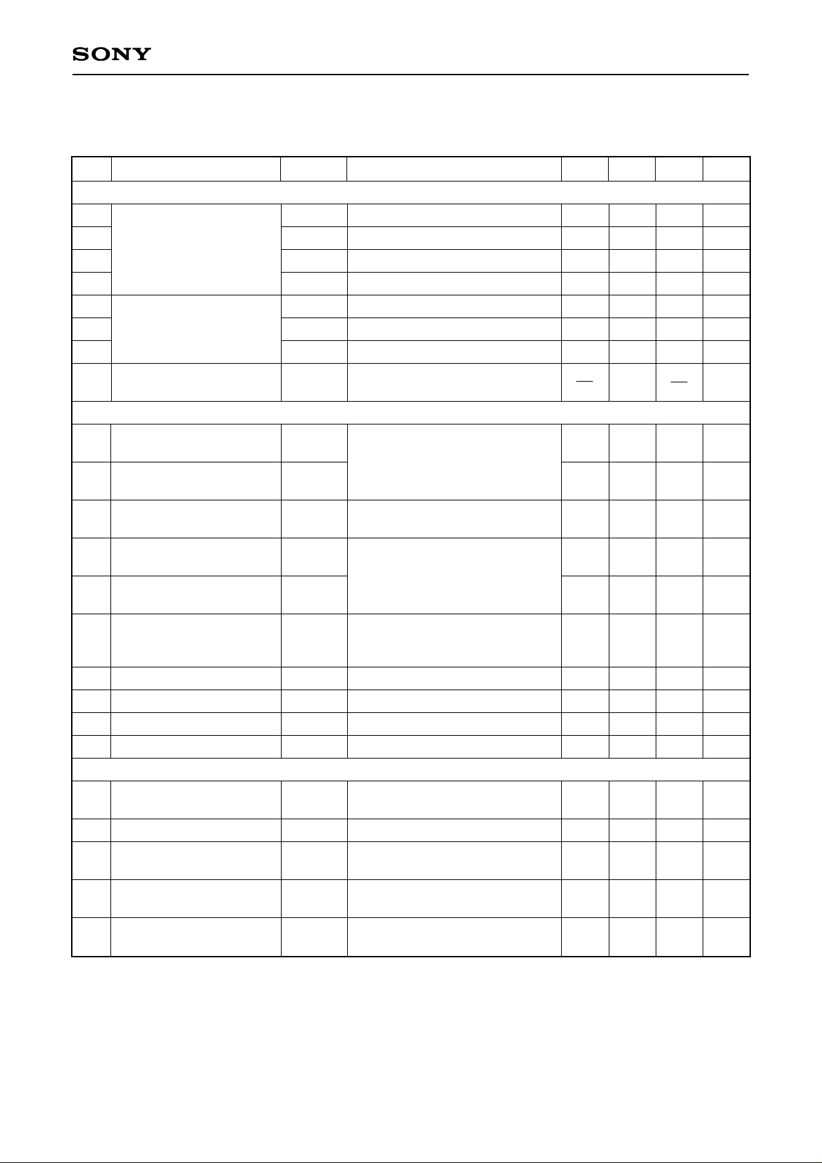
Electrical Characteristics
(Unless otherwise specified; VCC = 5V, VEE = –3V, Ta = 25°C, CAP = 0.1µF, RS = 7.5kΩ)
No. Item Symbol Measurement conditions Min. Typ. Max. Unit
1-1
1-2
1-3
1-4
1-5
1-7
1-8
1-9
2-1
2-2
2-3
2-4
2-5
2-6
3-1
3-2
3-3
3-4
4-1
4-2
5-1
5-2
6
VCC power supply current
VEE power supply current
Bank write mode
TTL input
low input voltage
TTL input
high input voltage
TTL input
input current
Serial interface input
low input voltage
Serial interface input
high input voltage
Serial interface input
input current
P-ECL common voltage
P-ECL differential voltage
P-ECL high voltage
P-ECL input current
Bank write enable voltage
Bank write enable current
FLT output low voltage
FLT output high voltage
BHV gain accuracy
ISP1
IID1
IRE1
IWR1
IID2
IRE2
IWR2
ICCBW
VIL
VIH
ITTL
VSIL
VSIH
VST
VPC
VPD
VPH
IWD
VSEH
ISEH
VFLTL
VFLTH
EBHV
Sleep mode
Idle mode
Read mode
Write mode
Idle mode
Read mode
Write mode
ICCBW = 17 + 17 × N + IW × N
IW = 29.5mA
TTL input; R/XW
Internal pull-up resistor
High voltage: 5V
Low voltage: 0V
Serial input;
SDATA, SCLK, SDEN
High voltage: 3.3V
Low voltage: 0V
Pull-down resistor: 14kΩ
(VH + VL)/2
(VH – VL)
Input voltage: 4V
Open collector output
External resistance = 2.4kΩ
Open collector output
External resistance = 2.4kΩ
VBHV = VCC – 4 × IB × (RMR + 5.5Ω)
IB = "111", RMR = 50Ω
0
2.0
–200
2.35
–500
1.55
0.2
–20
VCC
+ 1.2
6
4.5
–8
2.15
22
37
98
10
10
10
111
2.85
29
48
130
13
13
13
0.8
VCC
+ 0.3
200
0.8
500
VCC
1.5
VCC
20
VCC
+ 1.4
14
0.8
8
mA
mA
mA
mA
mA
mA
mA
mA
V
V
µA
V
V
µA
V
V
V
µA
V
mA
V
V
%
Power Dissipation IW = 29.5mA, IB = 5.9mA
Digital Inputs
Power Dissipation IW = 29.5mA, IB = 5.9mA
 Loading...