

Sony CXA3510N Datasheet

—1—
E99201
Sony reserves the right to change products and specifications without prior notice. This information does not convey any license by
any implication or otherwise under any patents or other right. Application circuits shown, if any, are typical examples illustrating the
operation of the devices. Sony cannot assume responsibility for any problems arising out of the use of these circuits.
4ch. Read/Write Amplifier for
Thin Film Head of Hard Disk Drive
CXA3510N
Description
The CXA3510N is a Read/Write Amplifier for the
thin film head of hard disk drive and designed to
handle up to 4 channel heads.
Features
• Operate on single +5 V power supply
• Low power consumption
Read : 85 mW
Write : 115 mW + IW × 5
Idle : 8 mW
• Designed for two terminal thin-film or MIG heads
• Read amplifier emitter follower output featuring
360 times gain (typ).
• Differential input capacitance for Read : 6pF (typ)
• Input noise : 0.47 nV / √ Hz (typ)
• Write current range : 5 to 15 mA
• Differential Head voltage swing : 9 Vp-p (typ)
• IW Rise / Fall times : 3.7 ns (typ)
(LH=540 nH, RH=25 Ω, IW=10 mA)
• Differential P-ECL write data input
• Built-in write unsafe detection circuit.
• Built-in Servo write function (2/4 ch).
• Built-in IC protection circuit for short of head to
GND.
• Read data outputs are high impedance in write
mode.
• Unselected head voltage is GND potential.
• Built-in supply voltage monitor circuit prohibits
incorrect write during power on or abnormal
voltage.
• Self switching damping resistance (RD = 360 Ω).
Function
Read, Write and Write unsafe detection for HDD,
power supply ON/OFF detection.
Structure
Bipolar silicon monolithic IC
20 pin SSOP (Plastic)
Absolute Maximum Ratings (Ta=25 °C)
• Supply voltage VCC 6V
•Write current IW 20 mAo-p
• Operating temperature Topr –20 to +75 °C
• Storage temperature Tstg –55 to +150 °C
• Allowable power dissipation
PD 620 mW
• WUS/SE pin input current
ISEH 15 mA
Recommended Operating Conditions
• Supply voltage VCC 5.0 V±10 %
• Write current IW 5 to 15 mAo-p
For the availability of this product, please contact the sales office.
—2—
CXA3510N
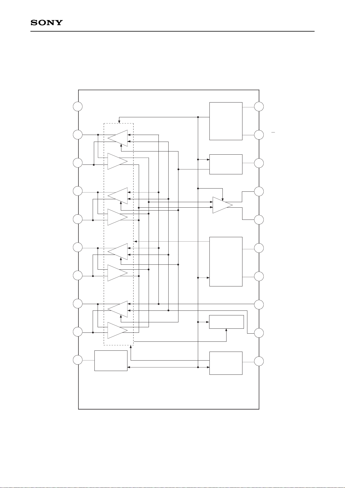
POWER
ON/OFF
DETECTOR
DRIVER
AMP
AMP
DRIVER
MODE
CONTROL
WRITE
CURRENT
SOURCE
AMP
HEAD
SELECT
WRITE
UNSAFE
DETECTOR
IC
PROTECTOR
H0X
H0Y
H1X
H1Y
H2X
H2Y
H3X
H3Y
GND
V
CC
R/W
WC
RDY
RDX
HS0
HS1
WDX
WDY
WUS/SE
XCS
AMP
DRIVER
DRIVER
8
1
2
3
4
5
6
7
9
10
20
14
15
16
17
18
19
13
12
AMP
11
Block Diagram and Pin Configuration
—3—
CXA3510N
Pin Description
No.
1
2
3
4
5
6
7
8
9
10
11
12
13
Symbol
GND
H0X
H0Y
H1X
H1Y
H2X
H2Y
H3X
H3Y
VCC
WUS/SE
WDY
WDX
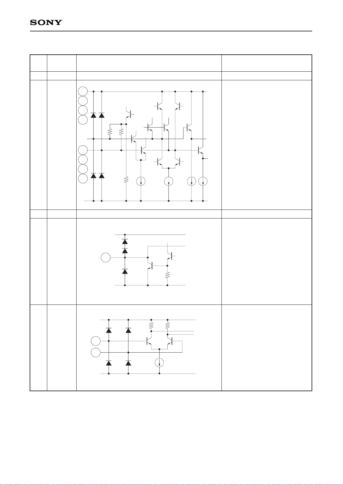
Equivalent circuit
2k 2k
VCC
GND
2
4
6
8
3
5
7
9
100k
Description
Head.
4 channels provided.
5 V power supply.
Write unsafe detection output /
Servo Enable signal input.
Differential P-ECL write data
input.
VCC
GND
11
VCC
GND
12
13
—4—
CXA3510N
No.
14
15
16
17
18
19
20
Symbol
HS1
HS0
RDX
RDY
WC
R/W
XCS
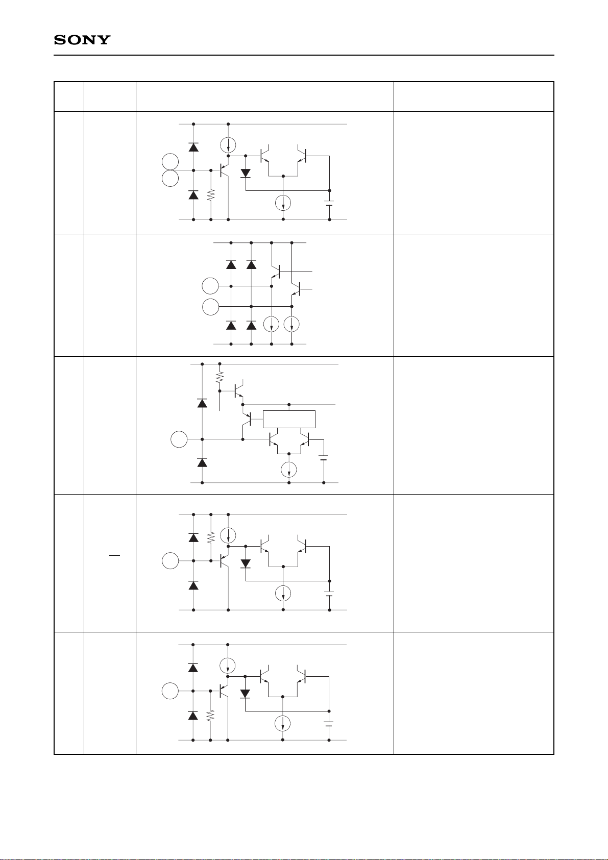
Equivalent circuit
VCC
GND
14
15
100k
2.1V
VCC
GND
16
17
VCC
GND
18
2.5V
VCC
GND
100k
2.1V
19
VCC
GND
100k
2.1V
20
Description
Head select signal input.
Selects one of 4 heads according
to Table 2.
Read Amplifier output.
A setting resistor for the write
current value is connected
between this pin and GND.
Read/Write signal input
At “High” : Read,
at “Low” : Write.
Power save signal input
At “High” : Power saving.
—5—
CXA3510N
Electrical Characteristics (Unless otherwise specified, VCC=5 V, Ta=25 °C, Write current IW=15 mA)
Refer to Fig.1
No.
1-1
1-2
1-3
2-1
2-2
2-3
2-4
2-5
2-6
2-7
2-8
3-1
3-2
Item
Current consumption
for Read
Current consumption
for Write
Current consumption
for idle
Digital input “Low”
input voltage
Digital input “High”
input voltage
Digital input “Low”
input current
Digital input “High”
input current
Write data input
“Low” input voltage
Write data input
“High” input voltage
Write data
input current
Unselected
head voltage
Write unsafe output
saturation voltage
Write unsafe output
leak current
Symbol
I
CCR
ICCW
ICCI
VIL
VIH
IIL
IIH
VWDL
VWDH
IWD
Vunsel
VWUS
IWUS
SW conditions
1 2 3 4 5 6 7 8 9 10 11 12 13 14
a a a a a b a a b a a b b a
a a a a a b a a b a a b a a
a a a a a b a a b a a b a b
a a a a a b a a b a a b a a
a a a a a b a a b b b b b b
a a a a a b a a b a a b a a
b a a a b b a c c c c b a a
a a a a a a a a b a a b a a
Measurement conditions
Test point : l
2
Test point : l2
Test point : I2
Digital input :
Pins 14, 15, 19, 20
“High” applied voltage : 5 V
“Low” applied voltage : 0 V
Test point : l6, l7, l8, I9
Input voltage : 4 V
Output current : 1 mA
Test point : V1
Test point : l
3
Min. Typ. Max. Unit
11 17 26 mA
16 22 36
mA
+IW +IW +IW
1.0 1.6 2.3 mA
0.8 V
2.0 V
–100 µA
100 µA
VWDH VWDH
V
–2.0 –0.25
VCC VCC
V
–1.1 –0.4
50 µA
0.3 V
0.5 V
50 µA
—6—
CXA3510N
No.
4
5-1
5-2
5-3
5-4
6-1
6-2
7
8
Item
Supply power
ON/OFF detector
threshold voltage
Write current
setting range
Write current voltage
Write current gain
Write current
setting constant
WUS/SE voltage
WUS/SE sink current
Read amplifier
differential voltage gain
Frequency band
width (–3 dB)
Symbol
V
TH
IW
VWC
AW
KW
VSEH
ISEH
AV
BW
Measurement conditions
When V
CC is lowered from 5 V in
Write mode and IW does not flow
anymore, VCC voltage is set to
VTHOFF. When VCC is raised from 3
V and IW starts to flow, VCC voltage
is set to VTHON.
IW=AW • VWC/RWC
IW=KW/RWC
Servo write enabled
Servo write enabled
Input voltage SG1 :
1 mVp-p, 300 kHz
Load resistance (RDX, RDY) :
1 kΩ
Test point : V4 [Vp-p]
AV =
V4
SG1
Frequency at which AV lowers
by 3 dB
Min. Typ. Max. Unit
3.4 3.9 4.3 V
5 15 mAo-p
2.25 2.5 2.75 V
18 20 22
mA/mA
45 50 55
VCC VCC V
+1.5 +1.6
5 14 mA
305 360 415 V/V
100 140 MHz
SW conditions
1 2 3 4 5 6 7 8 9 10 11 12 13 14
b a a a a a b a a b a b a a
a a a a a b a a b a a b a a
b a a a a b a a b a a b a a
b a a a a b b a b a a b a a
b a a a c b a a b a a b b a
b a a a c b a a b a a b b a
 Loading...