Sony CXA3329ER Datasheet

CXA3329ER
Analog Signal Processor TX-IF IC for W-CDMA Cellular Phones
Description
The CXA3329ER is an analog signal processor
TX-IF IC for the W-CDMA cellular phones. This IC
contains voltage-controlled gain control amplifier and
quadrature modulator .
Features
• Gain control amplifier with a linear and wide gain
variable range
• I-Q quadrature modulator
• Power saving switch
• Low voltage operation (2.7 to 3.3V)
• Small package (24-pin VQFN)
Applications
Analog signal processor TX-IF IC for the W-CDMA
cellular phones
24 pin VQFN (Plastic)
Preliminary
Structure
Bipolar silicon monolithic IC
Absolute Maximum Ratings
• Supply voltage Vcc –0.3 to +5.5 V
• Operating temperature Topr –55 to +125 °C
• Storage temperature Tstg –65 to +150 °C
Recommended Operating Conditions
• Supply voltage Vcc 2.7 to 3.3 V
• Operating temperature Ta –25 to +85 °C
Sony reserves the right to change products and specifications without prior notice. This information does not convey any license by
any implication or otherwise under any patents or other right. Application circuits shown, if any, are typical examples illustrating the
operation of the devices. Sony cannot assume responsibility for any problems arising out of the use of these circuits.
– 1 –
PE00Y17-PS

Block Diagram
CXA3329ER
CC
PS
VCONT
AGCV
CC2
AGCGND2
OUTX
OUT
19
20
21
22
23
24
NC
GCA control
NC
MODV
MODGND
15 14161718 13
Switch
PVCC
1/4
1/2
PGND
12
11
10
9
8
7
NC
GND4
Local IN
NC
NC
Local SW
4 5321 6
I
AGCVCC1
AGCGND1
IX
Q
QX
– 2 –

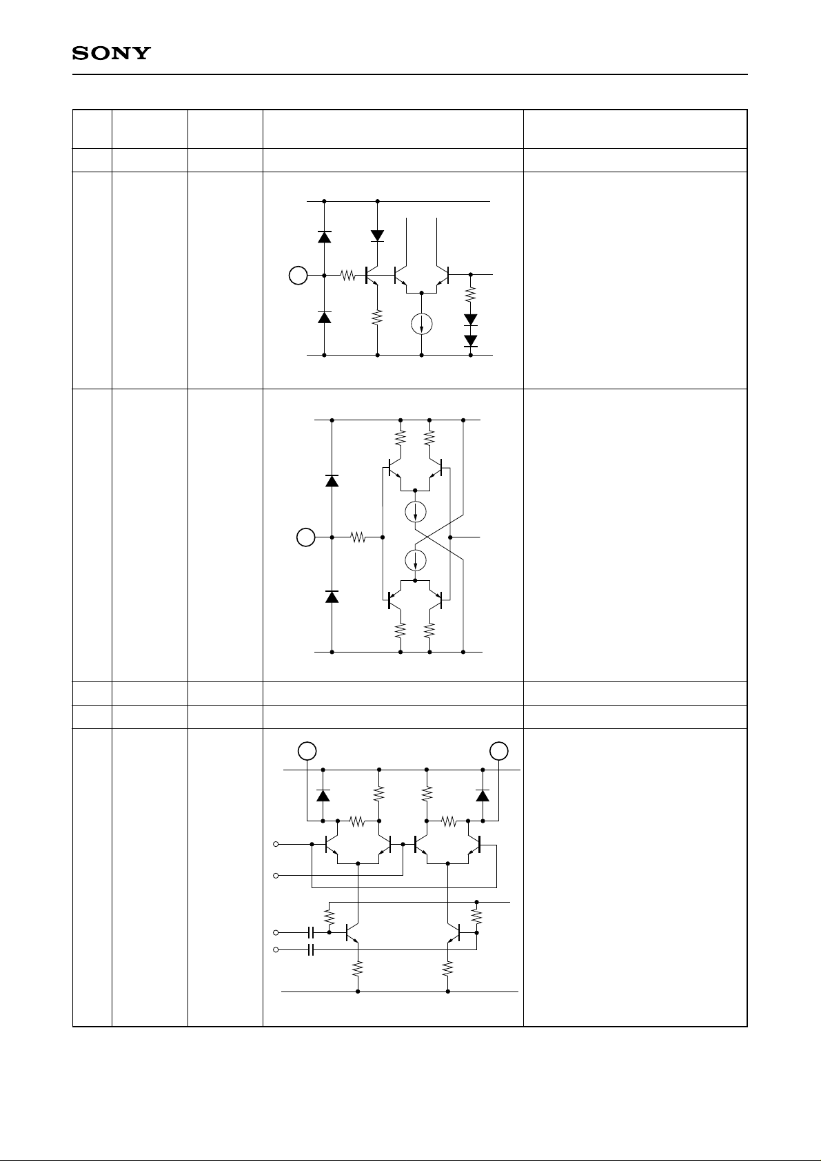
Pin Description
CXA3329ER
Pin
No.
Symbol Equivalent circuit Description
Typical pin
voltage [V]
1 AGCVCC12.85
2 AGCGND1 0
3, 4
5, 6
I, IX
Q, QX
1.425
7 Local SW —
Positive power supply.
Ground.
MODVCC
53
64
30k
7
150
150
2k
MODGND
PV
I, Q inputs.
Applies a bias voltage from the
external source.
CC
Frequency division value selection.
High: 1/4 frequency division
Low: 1/2 frequency division
Open: Low
PGND
8, 9 NC — No connection.
PV
CC
10
10 Local IN — Local input.
50
11
12
13
14
15
16
GND4
NC
PGND
PVCC
MODGND
MODVCC
0
—
0
2.85
0
2.85
0.5k
PGNDGND4
2k
2k
Ground.
No connection.
Ground.
Positive power supply.
Ground.
Positive power supply.
– 3 –

CXA3329ER
Pin
No.
17, 18
19 PS
Symbol Equivalent circuit
Typical pin
voltage [V]
NC
40k
60k
8k 8k
—
19
Description
No connection.—
AGCVCC2
Power saving mode switch input.
High: Active mode
Low: Power saving mode
AGCGND2
AGCVCC2
21 AGCV
22
AGCGND2
2324OUTX
OUT
CC2
2.85
—
20
23 24
20k
6k 6k
AGCGND2
AGCVCC1
25 25
890 890
Gain control voltage input.20 VCONT —
Positive power supply.
Ground.0
IF signal differential output.
AGCGND1
– 4 –

Input Conditions for Each Pin
CXA3329ER
Pin
No.
3, 4,
5, 6
3, 4,
5, 6
3, 4,
5, 6
7
7
10
10
19
19
20
Item Symbol
I/Q bias voltage
I/Q input voltage
I/Q band width
Local switch voltage-High
Local switch voltage-Low
Local frequency
Local input level
PS voltage-High
PS voltage-Low
Control voltage range
VBIQ
VIQ
BWIQ
VLSH
VLSL
fLO
LO
VPSH
VPSL
VCN
Conditions
Differential input
Min.
1.35
—
—
2.5
0
—
–18
2.0
0
0
Typ.
1.425
0.4
—
760
–15
Max.
1.65
1
5
VCC
0.8
—
–12
VCC
0.8
VCC
Unit
V
Vp-p
MHz
V
V
MHz
dBm
V
V
V
– 5 –
 Loading...