Sony CXA3304N Datasheet

—1—
E98X40-TE
Sony reserves the right to change products and specifications without prior notice. This information does not convey any license by
any implication or otherwise under any patents or other right. Application circuits shown, if any, are typical examples illustrating the
operation of the devices. Sony cannot assume responsibility for any problems arising out of the use of these circuits.
Absolute Maximum Ratings (Ta=25 °C)
• Supply voltage VCC 14.0 V
• Operating temperature Topr –30 to +100 °C
• Storage temperature Tstg –65 to +150 °C
• Allowable power dissipation
PD 300 mW
Operating Condition
Supply voltage VCC 2.5 to 5.5 V
Description
The CXA3304N is an IF signal processing IC for
the ETC car-mounted system which employs the
newest bipolar process.
Features
• Low current consumption 7.8 mA
(typ. at VCC=3.0 V)
• Small package 16-pin SSOP
• 40 MHz IF amplifier
• RSSI function
• RSSI buffer
• Peak hold circuit for carrier detection
• Comparator for carrier detection
• Comparator for data output waveform shaping
• Sleep mode supported
Application
ETC car-mounted system
Structure
Bipolar silicon monolithic IC
IF IC for ETC
16 pin SSOP (Plastic)
CXA3304N

—2—
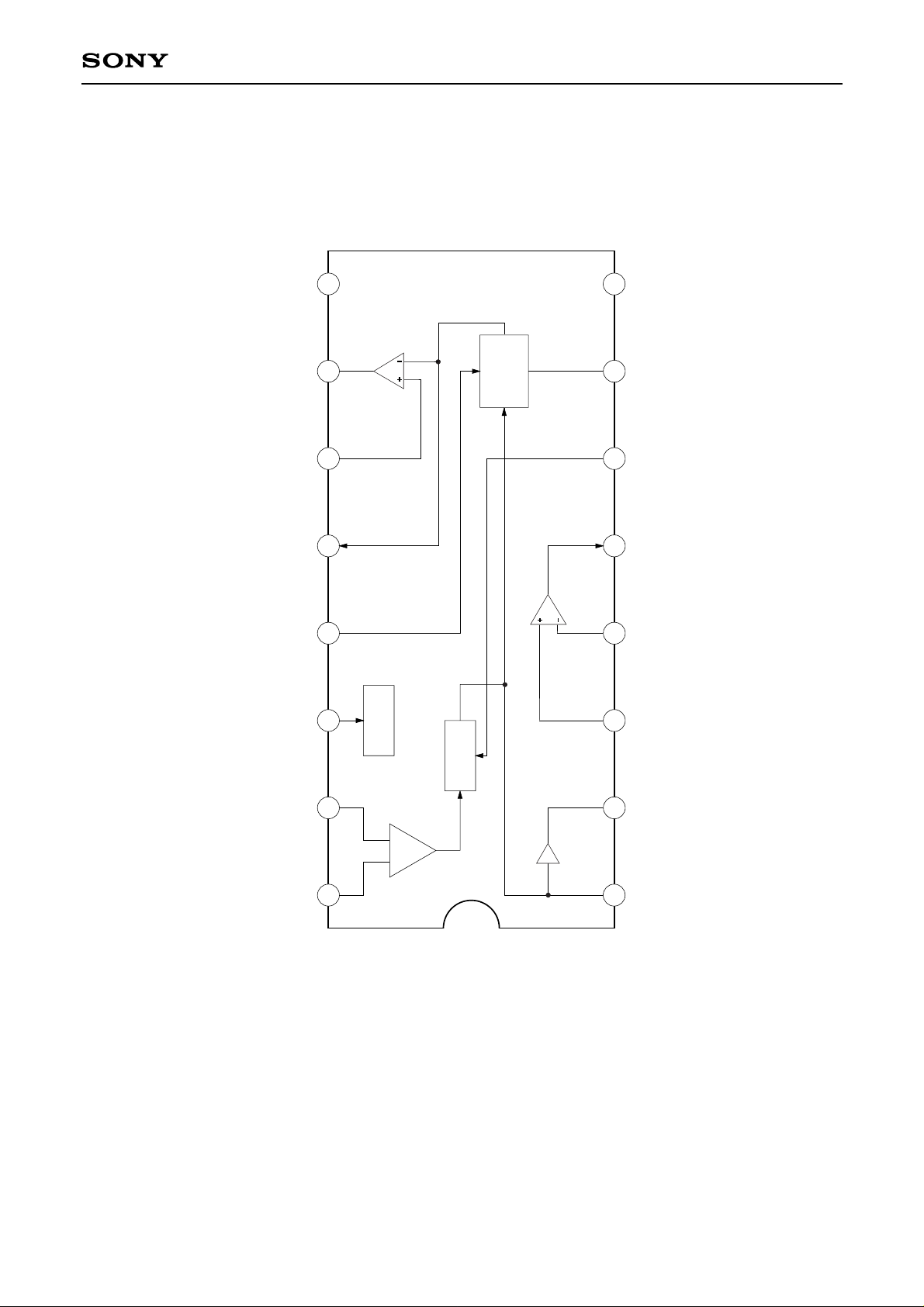
CXA3304N
1
2 3 4 5 6
7
8
9
10111213141516
LIM
BIAS
RSSI
COMP1
COMP2
PEAK
HOLD
VCC
CARRIER SENSE
VREF
RSSI PEAK
PEAK HOLD
POWER SAVE
XIF IN
IF IN
RSSI OUT
BUFFER OUT
COMP IN
REF IN
DATA OUT
RSSI REF
HOLD CAP
GND
Block Diagram and Pin Configuration

—3—
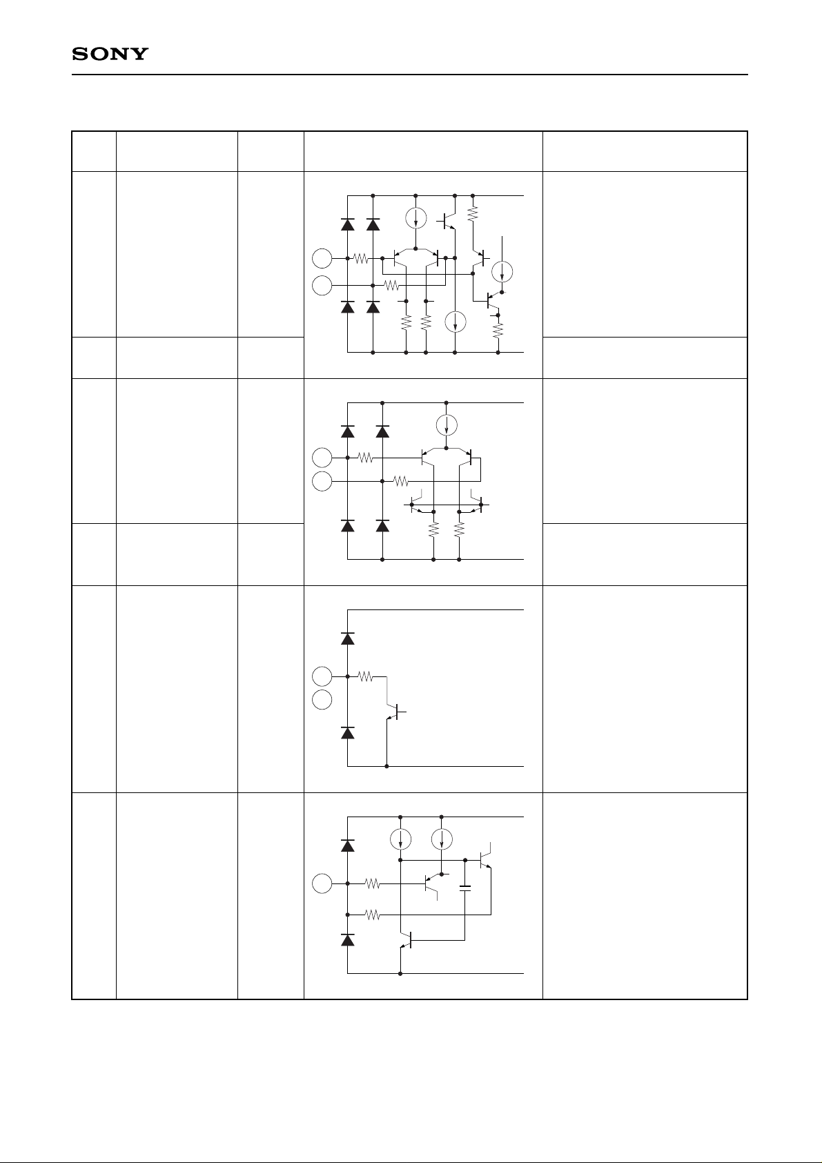
CXA3304N
Pin
Symbol
Pin
Equivalent circuit Description
No. voltage
1
2
3
4
5
10
6
RSSI OUT
BUFFER OUT
COMP IN
REF IN
DATA OUT
CARRIER SENSE
RSSI REF
—
—
—
—
—
0.2 V
RSSI output and RSSI buffer
input.
The current output is converted
to the voltage and it undergoes
the waveform shaping by the
external resistor and capacitor.
The input/output voltage range
is between 0.2 V to 1.4 V.
Buffer output which outputs the
RSSI voltage.
Comparator input.
Comparator reference voltage
input.
Comparator output.
Open collector.
Connects the resistor which
determines the output current
characteristics for the RSSI
circuit.
GND
10
5
VCC
62
VCC
GND
6
124
124
GND
3
4
VCC
124
124
1
2
VCC
GND
124
124
Pin Description

—4—
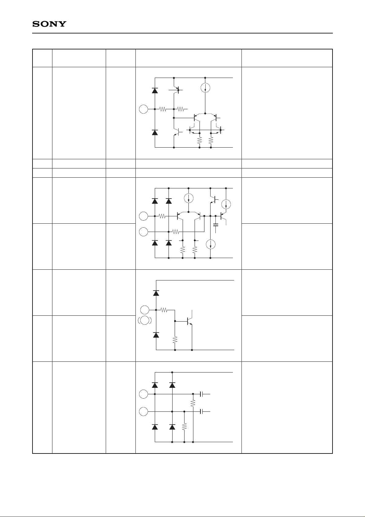
CXA3304N
Pin
Symbol
Pin
Equivalent circuit Description
No. voltage
7
8
9
11
12
13
14
15
16
HOLD CAP
GND
VCC
VREF
RSSI PEAK
PEAK HOLD
POWER SAVE
XIF IN
IF IN
—
—
—
—
—
—
—
0 V
Connects the external capacitor
which determines the peak hold
time constant.
The bias current of the internal
buffer circuit flows even in hold
mode.
Ground.
VCC.
Input of voltage which is the
threshold value of the carrier
sense comparator.
RSSI peak voltage output.
This is also connected to the
input pin for the carrier sense
comparator.
Peak hold circuit control.
Peak hold for low;
reset operation for high.
Power saving control.
Sleep mode for low;
IC operation for high.
IF signal input.
It is input with DC coupled.
Input the IF signal via a
matching circuit.
GND
7
VCC
124
VCC
GND
11
12
124
124
GND
VCC
13
14
20k
(28k)
80k
(120k)
VCC
GND
15
16
1.5k
1.5k
 Loading...