

Sony CXA3275Q Datasheet

PLL/OSC/MIX IC for Digital Tuner
Description
The CXA3275Q is a monolithic tuner IC for single
conversion system digital broadcast tuners. This IC
integrates three sets of local oscillator and mixer
circuits (VHF Low Band/ VHF High Band/UHF Band),
an IF amplifier and a tuning PLL onto a single chip,
enabling further miniaturization of the tuner.
Features
• Balanced oscillators with low-phase noise and
excellent oscillation stability (UHF: 4 pins, VHF: 2 pins)
• High linearity mixer and IF amplifier
• IF output switchable between balanced and
unbalanced
• Low-phase noise PLL synthesizer
(3-wire bus format)
• Reference frequency programmable in 4 bits
• On-chip high voltage drive transistor for charge
pump
• On-chip 4-output band switch (PNP transistor
on/off)
• 40-pin QFP package
Applications
Digital CATV tuners
Structure
Bipolar silicon monolithic IC
Absolute Maximum Ratings (Ta = 25°C)
• Supply voltage Vcc, PLLVcc –0.3 to +6.0 V
IFVcc –0.3 to +6.0 V
• Storage temperature
Tstg –55 to +150 °C
• Allowable power dissipation
PD 1.58 W
(when mounted on a printed circuit board)
Operating Conditions
• Supply voltage Vcc, PLLVcc 4.5 to 5.5 V
IFVcc 4.5 to 5.5 V
• Operating temperature
Topr –40 to +80 °C
– 1 –
E00461-PS
Sony reserves the right to change products and specifications without prior notice. This information does not convey any license by
any implication or otherwise under any patents or other right. Application circuits shown, if any, are typical examples illustrating the
operation of the devices. Sony cannot assume responsibility for any problems arising out of the use of these circuits.
CXA3275Q
40 pin QFP (Plastic)
This IC has pins whose electrostatic discharge strength is weak as a high-frequency process is used for this IC.
Take care when handling the IC.

– 2 –
CXA3275Q
Block Diagram and Pin Configuration
VLMIX VHMIX UMIX
UOSC
VHOSCVLOSC
IF Amp
Ref
OSC
Band
SW
Charge
Pump
Ref
Div.
Lock
Det
Program
Div.
Phase
Det
Bus
Interface
1
2 3 4 5 6 7 8 9 10
11
12
13
14
15
16
17
18
19
20
21
22
23
24
25
26
27
28
29
30
32
31
33
34
35
36
37
38
39
40
UIN2
Vcc
MIXOUT1
MIXOUT2
GND
IFIN1
IFIN2
RFGND
UOSCB1
UOSCE1
NC
BS4
BS3
BS2
BS1
VLIN1
VLIN2
VHIN1
VHIN2
UIN1
IFOUT1
IFOUT2
IFVcc
IFGND
VLOSC2
VLOSC1
VHOSC2
VHOSC1
UOSCB2
UOSCE2
PLLVcc
CP
VT
XI
XO
PLLGND
LOCK
SDA
SCL
CE
– 3 –
CXA3275Q
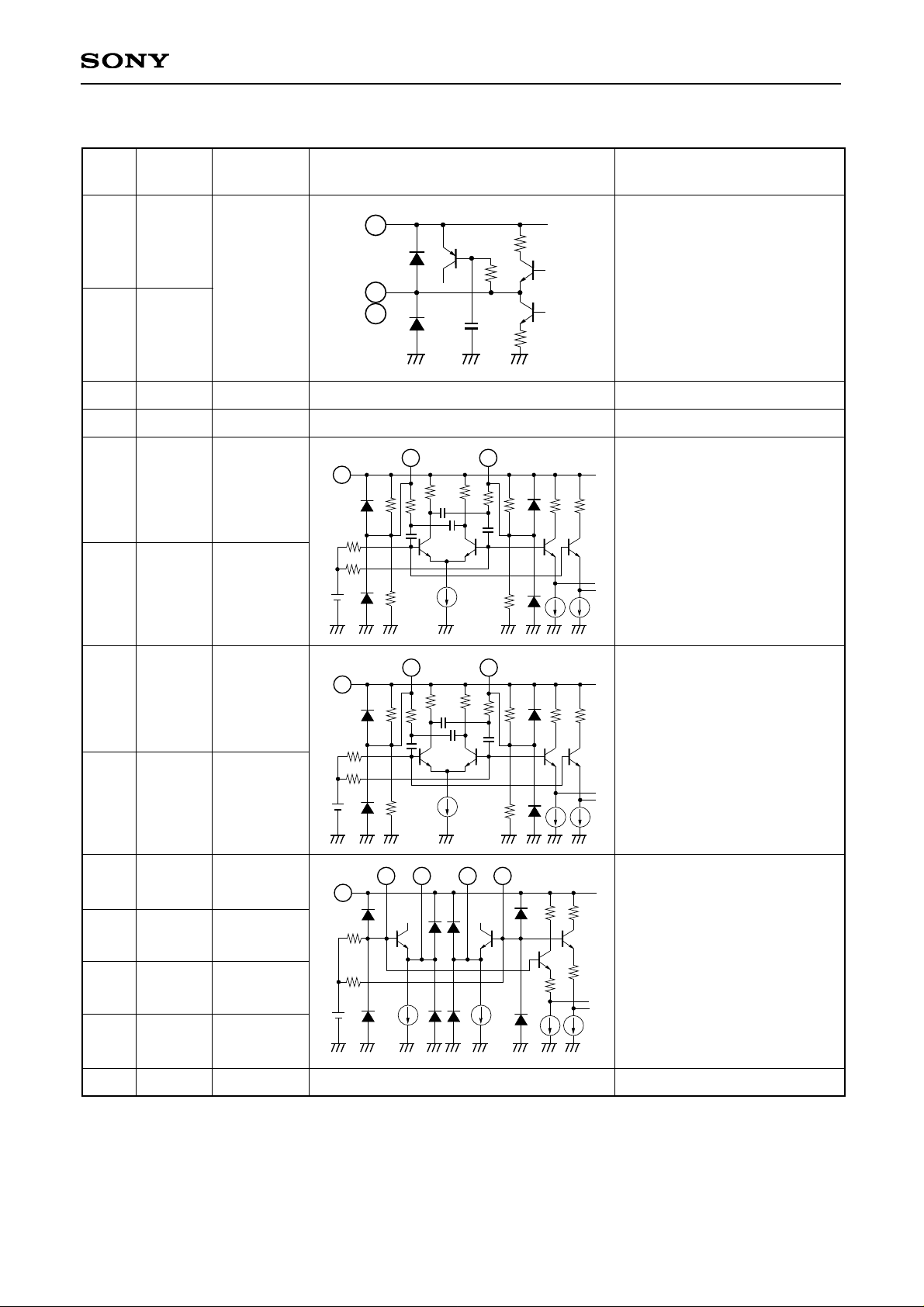
Pin Description and Equivalent Circuit
Pin
No.
Symbol
Pin voltage
[V]
1
IFOUT1
2
3
IFOUT2
IFVcc
2.5
—
5
VLOSC2
6
VLOSC1
2.5
2.5
Equivalent circuit Description
IF outputs.
IFOUT1 and IFOUT2 output a
balanced signal.
When taking a signal as an
unbalanced output, connect
the pin not used for output to
IFVCC. At this time the output
stage current is saved.
IF amplifier power supply.
4 IFGND
—
IF amplifier GND.
13
RFGND
—
Analog GND.
External resonance circuit
connection for VL oscillator.
40k
IFVcc
3
1
2
20k
20k
3k
3k
20k20k
Vcc
5
19
6
7
VHOSC2
8
VHOSC1
2.5
2.5
External resonance circuit
connection for VH oscillator.
20k
20k
3k
3k
20k20k
Vcc
7
19
8
12
UOSCB1
UHF: 2.2
VL/VH: 2.3
11
UOSCE1
UHF: 1.5
VL/VH: –
10
UOSCE2
UHF: 1.5
VL/VH: –
9
UOSCB2
UHF: 2.2
VL/VH: 2.3
External resonance circuit
connection for UHF oscillator.
3k
3k
Vcc
91910 11 12
– 4 –
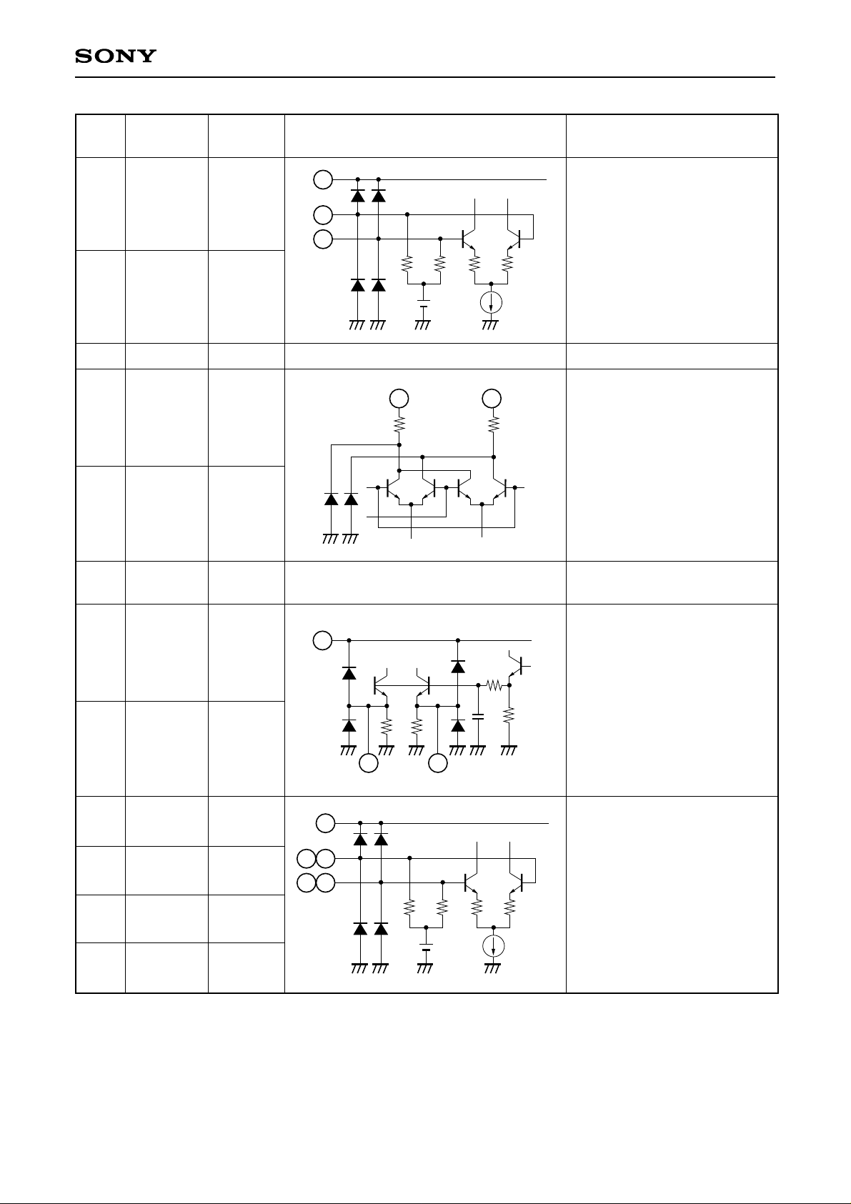
CXA3275Q
14
IFIN2
15
IFIN1
2.7
2.7
17
MIXOUT2
18 MIXOUT1
—
—
IF inputs.
16 GND
0
GND
19
Vcc
—
Band switch, mixer and local
oscillator circuit power supply.
Mixer outputs.
IFVcc
3
14
15
5k 5k
18 17
20 20
20
UIN2
21 UIN1
VL/VH: 0
UHF: 1.9
VL/VH: 0
UHF: 1.9
UHF inputs.
20
19
21
Vcc
25
VLIN1
VH: 3.16
VL: 3
UHF: 3.24
24
VLIN2
VH: 3.16
VL: 3
UHF: 3.24
23
VHIN1
VH: 3
VL: 3.16
UHF: 3.24
22
VHIN2
VH: 3
VL: 3.16
UHF: 3.24
VH and VL inputs.
Vcc
19
24
25
22
23
5k 5k
Pin
No.
Symbol
Pin voltage
[V]
Equivalent circuit Description
– 5 –
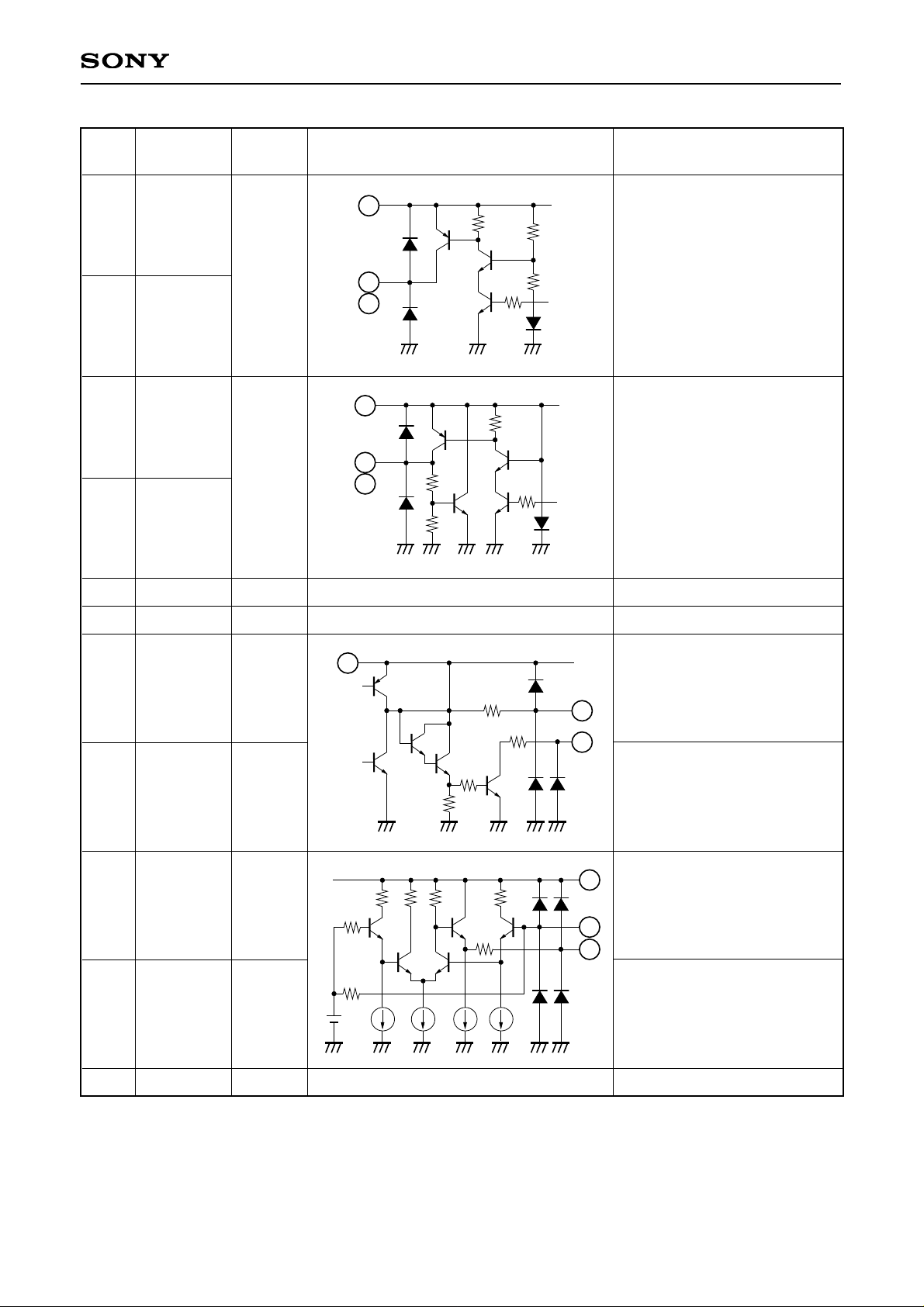
CXA3275Q
26
BS1
29 BS4
ON: 4.9
OFF: 0
Pin 26: Band switch 1 output.
Pin 29: Band switch 4 output.
The pin corresponding to the
band selected by the data
goes High.
20k
Vcc
19
26
29
27
BS2
28 BS3
ON: 4.9
OFF: 0
Pin 27: Band switch 2 output.
Pin 28: Band switch 3 output.
The pin corresponding to the
band selected by the data
goes High.
20k
70k
30k
Vcc
19
27
28
32
CP
33
VT
—
—
Charge pump output.
Connects the loop filter.
Transistor open collector
output for varicap diode drive.
Connects the loop filter.
50
33
32
31
PLLVcc
30 NC
—
NC.
31 PLLVcc
—
PLL VCC.
34
XI
35
XO
3.1
3.0
External reference clock input.
Connects the crystal when
used as a reference oscillator.
Connects the crystal when
used as a reference oscillator.
PLLVcc
31
500
34
35
36 PLLGND
— PLL GND.
Pin
No.
Symbol
Pin voltage
[V]
Equivalent circuit Description
– 6 –
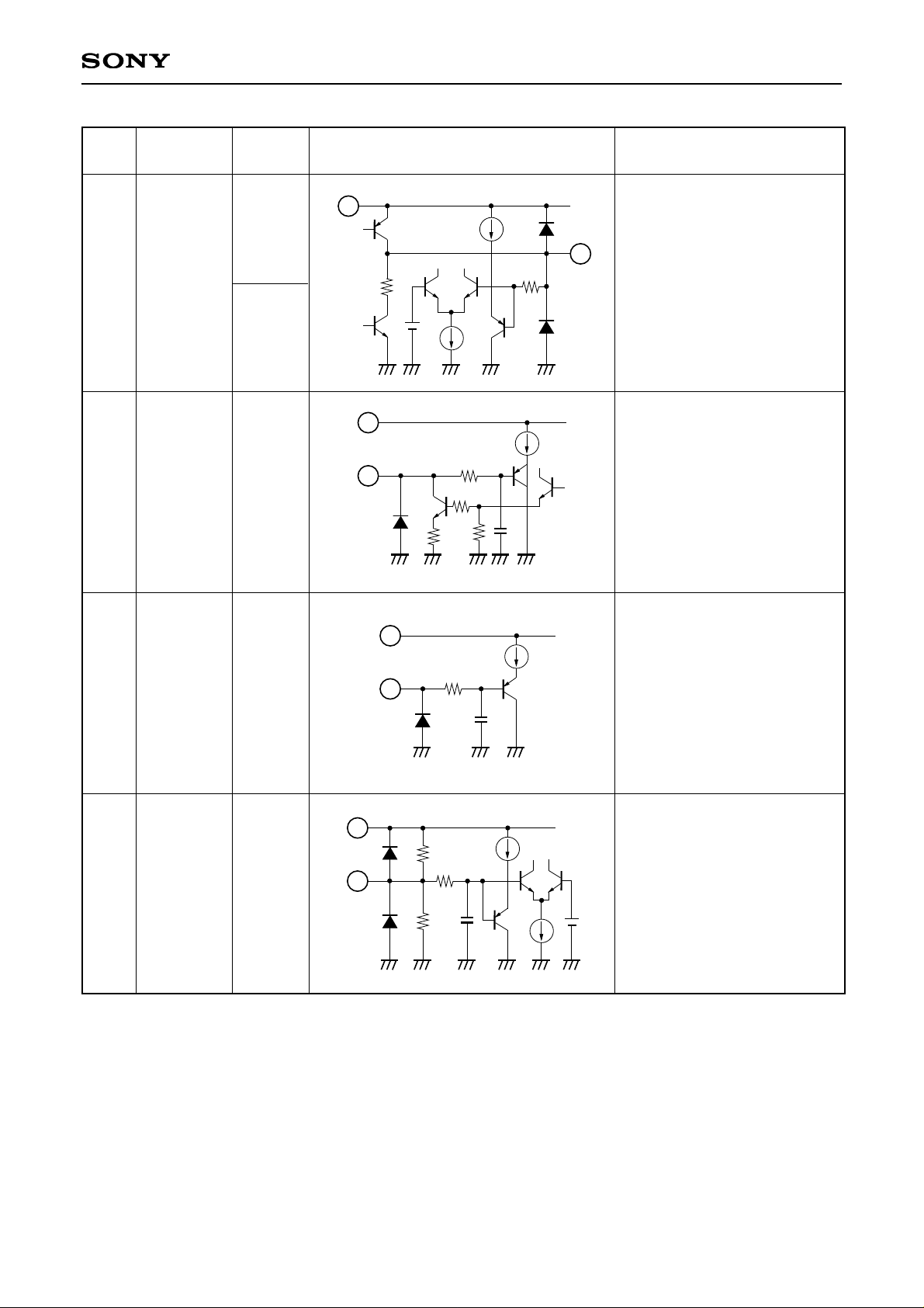
CXA3275Q
37
LOCK
5.0
(lock)
0.2
(unlock)
Lock detection.
High when locked, Low when
unlocked.
37
31
PLLVcc
38
SDA
—
Data input.
PLLVcc
20
5k
31
38
39
SCL
—
Clock input.
PLLVcc
5k
31
39
40
CE
1.25
(when open)
Enable pin.
PLLVcc
50k
150k
31
40
Pin
No.
Symbol
Pin voltage
[V]
Equivalent circuit Description

– 7 –
CXA3275Q
Electrical Characteristics (See the Electrical Characteristics Measurement Circuit.)
(Vcc = 5V, IFVcc = 5V, PLLVcc = 5V, Ta = 25°C)
Circuit Current
OSC/MIX/IF Amplifier Block
CG1-1
CG1-2
CG1-3
CG1-4
CG1-5
CG1-6
CG2-1
CG2-2
CG2-3
CG2-4
CG2-5
CG2-6
NF1
NF2
NF3
NF4
NF5
NF6
Conversion gain 1
∗1
(Unbalanced)
Conversion gain 2
∗
1, ∗2
(Balanced)
Noise figure
∗1, ∗3
(Unbalanced)
VL operation f
RF = 50MHz, fIF = 39MHz
VL operation fRF = 150MHz, fIF = 39MHz
VH operation fRF = 150MHz, fIF = 39MHz
VH operation fRF = 450MHz, fIF = 39MHz
UHF operation fRF = 450MHz, fIF = 39MHz
UHF operation fRF = 850MHz, fIF = 39MHz
VL operation fRF = 50MHz, fIF = 39MHz
VL operation fRF = 150MHz, fIF = 39MHz
VH operation fRF = 150MHz, fIF = 39MHz
VH operation fRF = 450MHz, fIF = 39MHz
UHF operation fRF = 450MHz, fIF = 39MHz
UHF operation fRF = 850MHz, fIF = 39MHz
VL operation fRF = 50MHz, fIF = 39MHz
VL operation fRF = 150MHz, fIF = 39MHz
VH operation fRF = 150MHz, fIF = 39MHz
VH operation fRF = 450MHz, fIF = 39MHz
UHF operation fRF = 450MHz, fIF = 39MHz
UHF operation fRF = 850MHz, fIF = 39MHz
18.5
19
19
19
23.5
24.5
25.5
26
26
26
30.5
31.5
21.5
22
22
22
26.5
27.5
28.5
29
29
29
33.5
34.5
15.5
15
15
15
10.5
10.5
25
25.5
25.5
25.5
30
31
32
32.5
32.5
32.5
37
38
18.5
18
18
18
13.5
13.5
dB
dB
dB
dB
dB
dB
dB
dB
dB
dB
dB
dB
dB
dB
dB
dB
dB
dB
Symbol
Item
Measurement conditions Min. Typ. Max. Unit
Symbol
Item
Measurement conditions Min. Typ. Max. Unit
Iccv1
Iccu1
Iccv2
Iccu2
Circuit current
During VHF operation
Unbalanced output
Band switch output open
During UHF operation
Unbalanced output
Band switch output open
During VHF operation
Balanced output
Band switch output open
During UHF operation
Balanced output
Band switch output open
80
85
91
100
113
120
130
137
145
151
170
177
mA
mA
mA
mA
 Loading...