

Sony CXA3268AR Datasheet
CXA3268AR
Driver/Timing Generator for Color LCD Panels
Description
The CXA3268AR is an IC designed to drive the color
LCD panels ACX300, ACX301, ACX302 and ACX703.
This IC greatly reduces the number of peripheral
circuits and parts by incorporating a RGB driver and
timing generator for video signals onto a single chip.
This chip has a built-in serial interface circuit and
electronic attenuators which allow various settings to
be performed by microcomputer control, etc.
Features
• Color LCD panel ACX300, ACX301, ACX302 and
ACX703 driver
• Supports NTSC and PAL systems
• Supports 16:9 wide display (letter box and pulse
elimination display)
• Supports Y/color difference and RGB inputs
• Supports OSD input (digital input)
• Power saving function
• Serial interface circuit
• Electronic attenuators (D/A converter)
• Trap and LPF (f0, fc variable)
• COMMON and PSIG output circuits
• Sharpness function
• 2-point γ correction circuit
• R, G, B signal delay time adjustment circuit
• D/A output pin (0 to 3V, 8 level output)
• Output polarity inversion circuit
• Supports AC drive for LCD panel during no signal
Applications
Compact LCD monitors, etc.
Absolute Maximum Ratings (Ta = 25°C)
• Supply voltage VCC16 V
VCC215 V
VCC315 V
VDD 5.5 V
• Analog input pin voltage
VINA (Pins 57, 58 and 59)
GND – 0.3 to VCC1 + 0.3 V
VINA (Pins 3, 69) VCC1V
VINA (Pin 30) 1.5 to VCC2 – 4 V
VINA (Pin 71) 0.9 Vp-p
VINA (Pins 70, 72) 0.8 Vp-p
• Digital input pin voltage
VIND (other than Pins 5, 10, 14, 15 and 16)
VSS – 0.3 to VDD + 0.3 V
VIND (Pins 5, 10) VSS – 0.3 to +5.5 V
• Common input pin voltage
VINAD (Pins 14, 15 and 16)
GND, VSS – 0.3 to +5.5 V
• Operating temperature
Topr –15 to +75 °C
• Storage temperature
Tstg –55 to +150 °C
• Allowable power dissipation
PD (Ta ≤ 25°C) 737 mW
Operating conditions
• Supply voltage
VCC1 – GND1 2.7 to 3.6 V
VCC2 – GND2 11.0 to 14.0 V
VCC3 – GND3 11.0 to 14.0 V
VDD – Vss 2.7 to 3.6 V
• Input voltage
SIG.C voltage
VSIG.C 5.0 to 6.5 V
RGB input signal voltage (Pins 70, 71 and 72)
∗1
VRGB 0 to 0.7 (0.5 typ.) Vp-p
Y input signal voltage (Pin 71)
∗2
VY 0 to 0.5 (0.35 typ.) Vp-p
R-Y input voltage (Pin 72)
∗2
VR-Y 0 to 0.49 (0.245 typ.) Vp-p
B-Y input voltage (Pin 70)
∗2
VB-Y 0 to 0.622 (0.311 typ.) Vp-p
∗1
During RGB input
∗2
During Y/color difference input
– 1 –
E99529B98-PS
Sony reserves the right to change products and specifications without prior notice. This information does not convey any license by
any implication or otherwise under any patents or other right. Application circuits shown, if any, are typical examples illustrating the
operation of the devices. Sony cannot assume responsibility for any problems arising out of the use of these circuits.
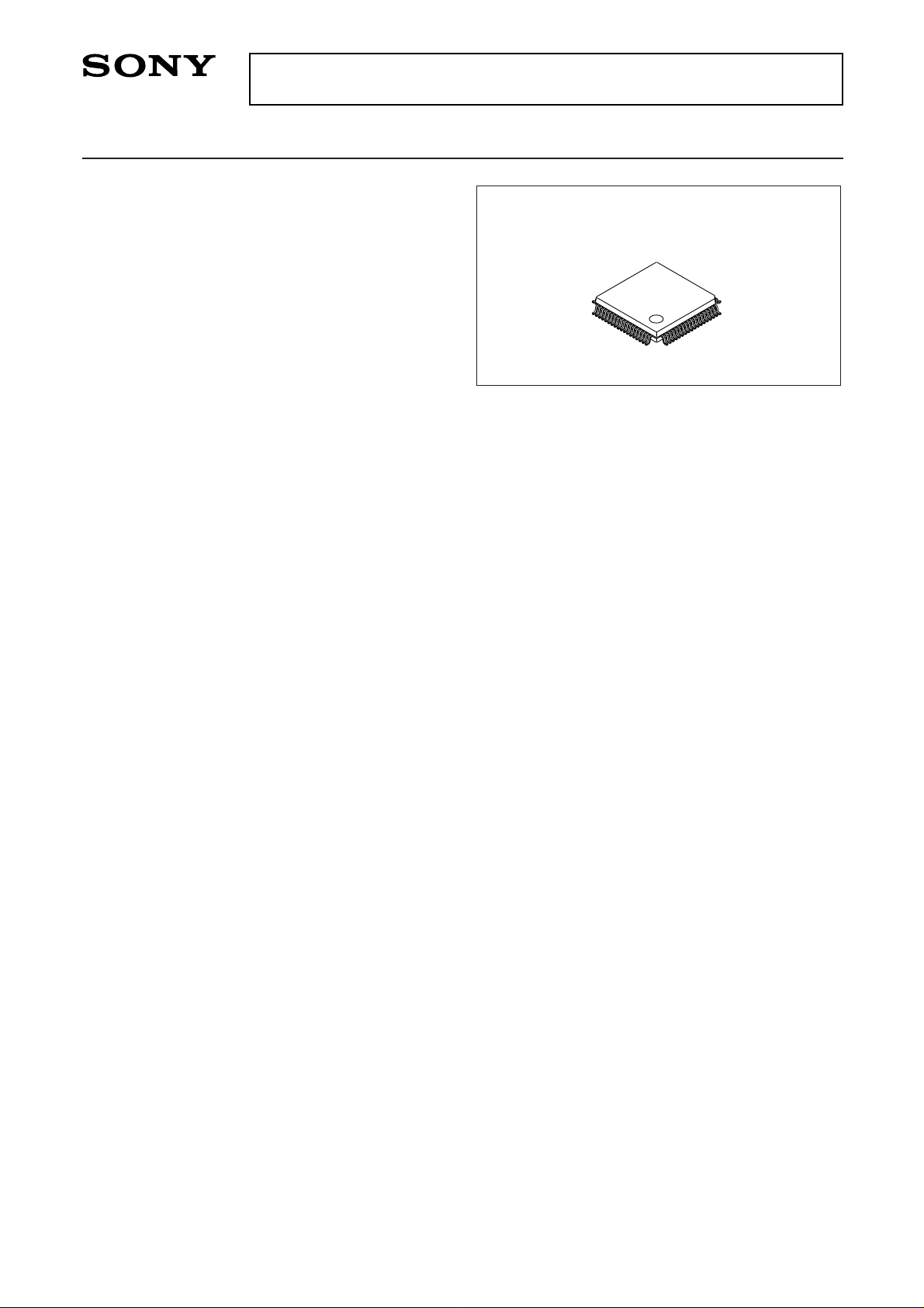
72 pin LQFP (Plastic)
– 2 –
CXA3268AR
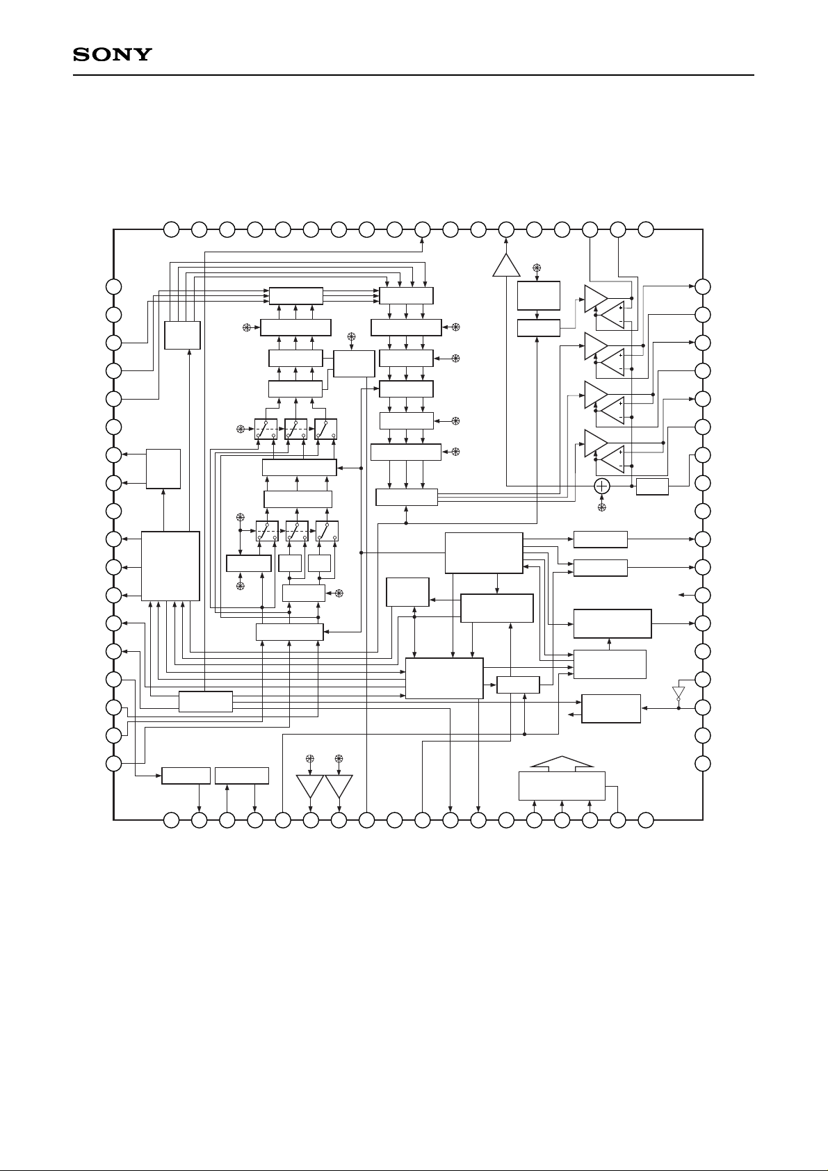
Block Diagram
1 2 3 4 5 6 7 8 9 10 11 12
13 14
15 16 17 18
19
20
21
22
23
24
25
26
27
28
29
30
31
32
33
34
35
36
37
38394041424344454647484950515253
54
55
56
57
58
59
60
61
62
63
64
65
66
67
68
69
70
71
72
Vss
FIL OUT
SYNC IN
SYNC OUT
CSYNC/HD
DA OUT
REF
F ADJ
GND1
VD
DWN
WIDE
TST1
SCK
SEN
SDAT
R INJECT
V
SS
G OUT
G DC DET
R OUT
R DC DET
B OUT
B DC DET
SIG.C
GND2
GND2
TST2
HDO
VDO
XCLR
RPD
Vss
CKI
CKO
V
DD
VDD
+3.0V
+3.0V
+3.0V
+3.0V
Vss
VssGND1Vss
MCK
V
DD
TST11
OSD B
OSD R
OSD G
NC
HCK1
HCK2
Vcc1
HST
EN
VCK
VST
RGT
FIL IN
B/B-Y
G/Y
DA
R/R-Y
Vss
Vss
TST10
TST9
TST8
TST7
TST6
TST5
NC
POF
TST4
GND3
COM
Vcc3
TST3
PSIG OUT
PSIG DC DET
Vcc2
CLK
CLP
Buf
+12.0V+12.0VGND3Vss Vss
S/P CONV
REGISTER DAC
PHASE
COMPARATOR
PLL
COUNTER
HSYNC DET
H SKEW DET
V CONTROL
V POSITION
PULSE
ELM
H.FILTER SYNC SEP
POL SW
MODE
HDO GEN
VDO GEN
S/H
S/H
GEN
HCK
GEN
OSD RGB
TRAP
LPF
CLAMP
FILTER
BIAS
HCOUNTER
HPULSE
GEN
POL SW
GAMMA
CLAMP
BLK-LIM
USER-BRIGHT
G R B
SUB-BRIGHT
CK
CONTROL
PSIGBRIGHT
Buf
PSIGBRT
U-BRT
MODE
LPF
FILTER
PIC-G
HUE
COLOR
PIC-F
CONT
SUB-BRT R
SUB-BRT B
γ 1 γ 2
WHITLIM
SUB-CONT R
SUB-CONT B
BLKLIM
COM-DC
REF
Buf
Buf
Buf
Buf
Buf
SIG.C
CONTRAST
G R B
CLAMP
MATRIX
DL1 DL1
PICTURE
HUE
V COUNTER
V SEP
– 3 –
CXA3268AR
Pin Description
Pin
No.
1
2
3
4
5
6
7
8
9
10
11
12
13
14
15
16
17
18
19
20
21
22
23
24
25
26
27
28
29
30
31
32
33
34
35
36
37
VSS
FIL OUT
SYNC IN
SYNC OUT
CSYNC/HD
DA OUT
REF
F ADJ
GND1
VD
DWN
WIDE
TST1
SCK
SEN
SDAT
R INJECT
VSS
VDD
VDD
CKO
CKI
VSS
RPD
XCLR
VDO
HDO
TST2
GND2
SIG.C
B DC DET
B OUT
R DC DET
R OUT
G DC DET
G OUT
VCC2
—
O
I
O
I
O
O
O
—
I
O
O
—
I
I
I
O
—
—
—
O
I
—
O
I
O
O
—
—
I
O
O
O
O
O
O
—
Digital 3.0V GND
H filter output (for using internal sync separation)
Sync separation circuit input (for using internal sync separation)
Sync separation circuit output (for using internal sync separation)
CSYNC/horizontal sync signal input
DAC output
Level shifter circuit REF voltage output for LCD panel
Trap f0 adjusting resistor connection
Analog 3.0V GND
Vertical sync signal input
Up/down inversion switching signal output
16:9 wide display switching pulse output
Test (Leave this pin open.)
Serial clock input
Serial load input
Serial data input
Serial block current controlling resistor connection
Digital 3.0V GND
Digital 3.0V power supply
Digital 3.0V power supply
Oscillation cell output
Oscillation cell input
Digital 3.0V GND
Phase comparator output
Power-on reset capacitor connection (timing generator block)
VDO pulse output
HDO pulse output
Test (Connect to GND.)
Analog 12.0V GND
R, G, B and PSIG output DC voltage adjustment
B signal DC voltage feedback circuit capacitor connection
B signal output
R signal DC voltage feedback circuit capacitor connection
R signal output
G signal DC voltage feedback circuit capacitor connection
G signal output
Analog 12.0V power supply
L
H
Symbol I/O Description
Input pin for
open status
– 4 –
CXA3268AR
Pin
No.
38
39
40
41
42
43
44
45
46
47
48
49
50
51
52
53
54
55
56
57
58
59
60
61
62
63
64
65
66
67
68
69
70
71
72
PSIG DC DET
PSIG OUT
TST3
VCC3
COM
GND3
TST4
POF
NC
TST5
TST6
TST7
TST8
TST9
TST10
VSS
VSS
VDD
TST11
OSD B
OSD R
OSD G
NC
HCK1
HCK2
VCC1
HST
EN
VCK
VST
RGT
FIL IN
B/B-Y
G/Y
R/R-Y
O
O
—
—
O
—
—
O
—
—
—
—
—
—
—
—
—
—
I
I
I
O
O
—
O
O
O
O
O
I
I
I
I
PSIG signal DC voltage feedback circuit capacitor connection
PSIG output
Test (Leave this pin open.)
Analog 12.0V COM (CS) power supply
Common pad voltage for LCD panel output (CS)
Analog 12.0V COM (CS) GND
Test (Leave this pin open.)
LCD panel power supply on/off (Leave this pin open when not using
this function.)
Test (Connect to GND.)
Test (Connect to GND.)
Test (Leave this pin open.)
Test (Leave this pin open.)
Test (Leave this pin open.)
Test (Leave this pin open.)
Digital 3.0V GND
Digital 3.0V GND
Digital 3.0V power supply
Test (Connect to GND.)
OSD B input
OSD R input
OSD G input
H clock pulse 1 output
H clock pulse 2 output
Analog 3.0V power supply
H start pulse output
EN pulse output
V clock pulse output
V start pulse output
Right/left inversion switching signal output
H filter input (for using internal sync separation)
B/B-Y signal input
G/Y signal input
R/R-Y signal input
Symbol I/O Description
Input pin for
open status
∗
DWN: DOWN SCAN and UP SCAN, RGT: RIGHT SCAN and LEFT SCAN
H: pull-up processing, L: pull-down processing
– 5 –
CXA3268AR
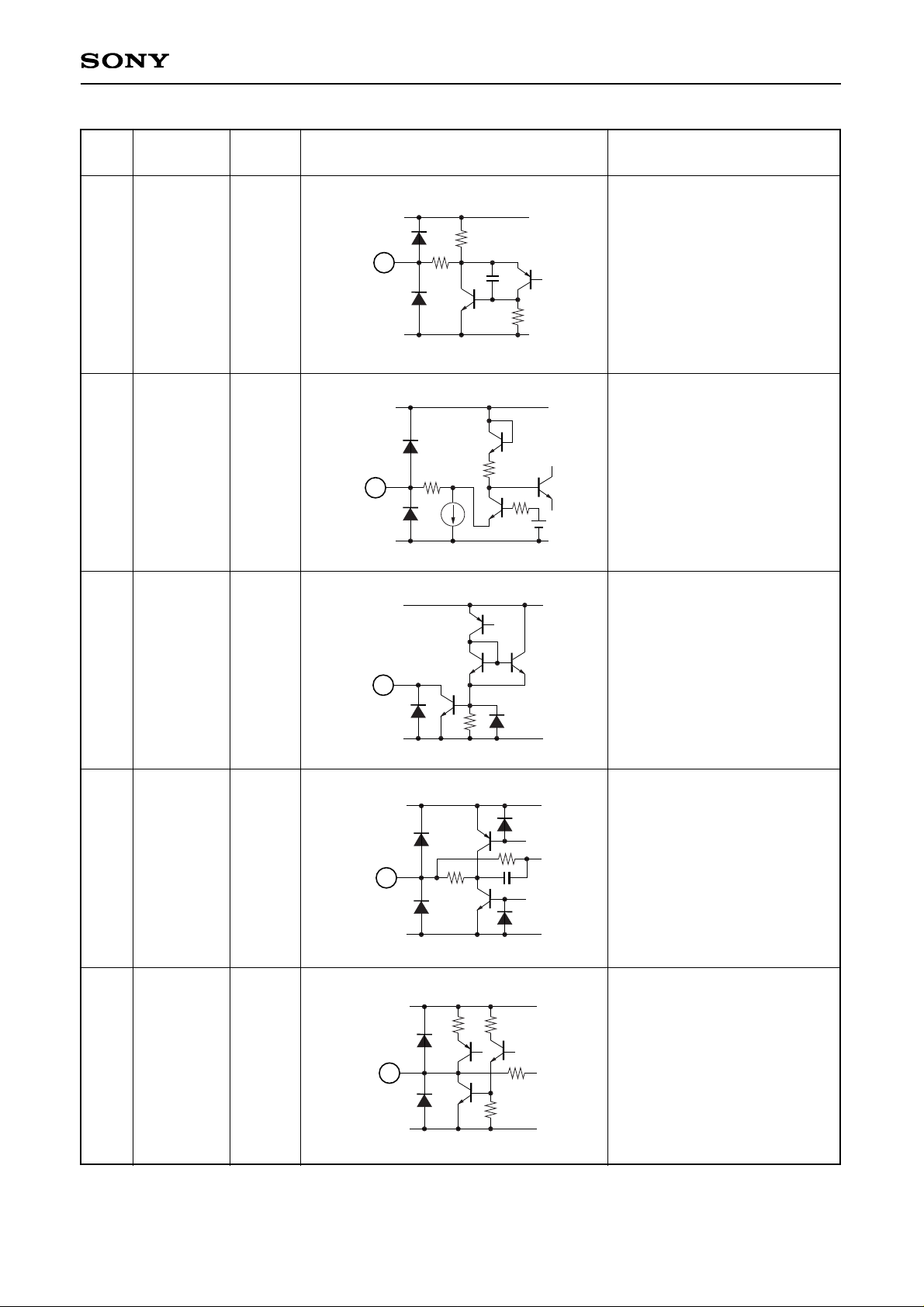
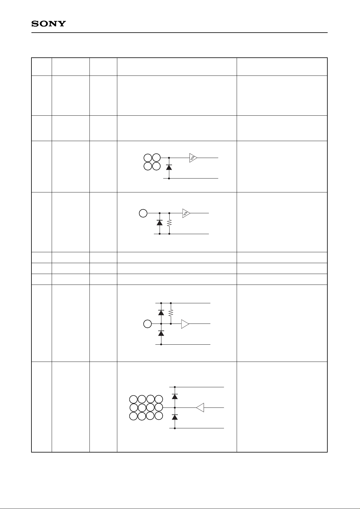
Analog Block Pin Description
Pin
No.
2 FIL OUT
Amplifies and outputs the sync
portion of the video signal input
to FIL IN (Pin 69).
Sync separation circuit input.
Inputs the FIL OUT (Pin 2)
output signal via a capacitor.
Sync separation output.
Positive polarity output in open
collector format.
DA output.
Outputs the serial data
converted to DC voltage. The
current driving capacity is
±1.0mA (max.).
REF output.
Outputs the serial data
converted to DC voltage. The
current driving capacity (sink)
is ±1.5mA (max.).
2.15V
1.1V
—
—
—
SYNC IN
SYNC OUT
DA OUT
REF
3
4
6
7
Symbol
Pin
voltage
Equivalent circuit Description
VCC1
23k
200
GND1
2
VCC1
200
GND1
3
VCC1
GND1
4
VCC1
50
50
GND1
6
VCC1
51k
GND1
7
– 6 –
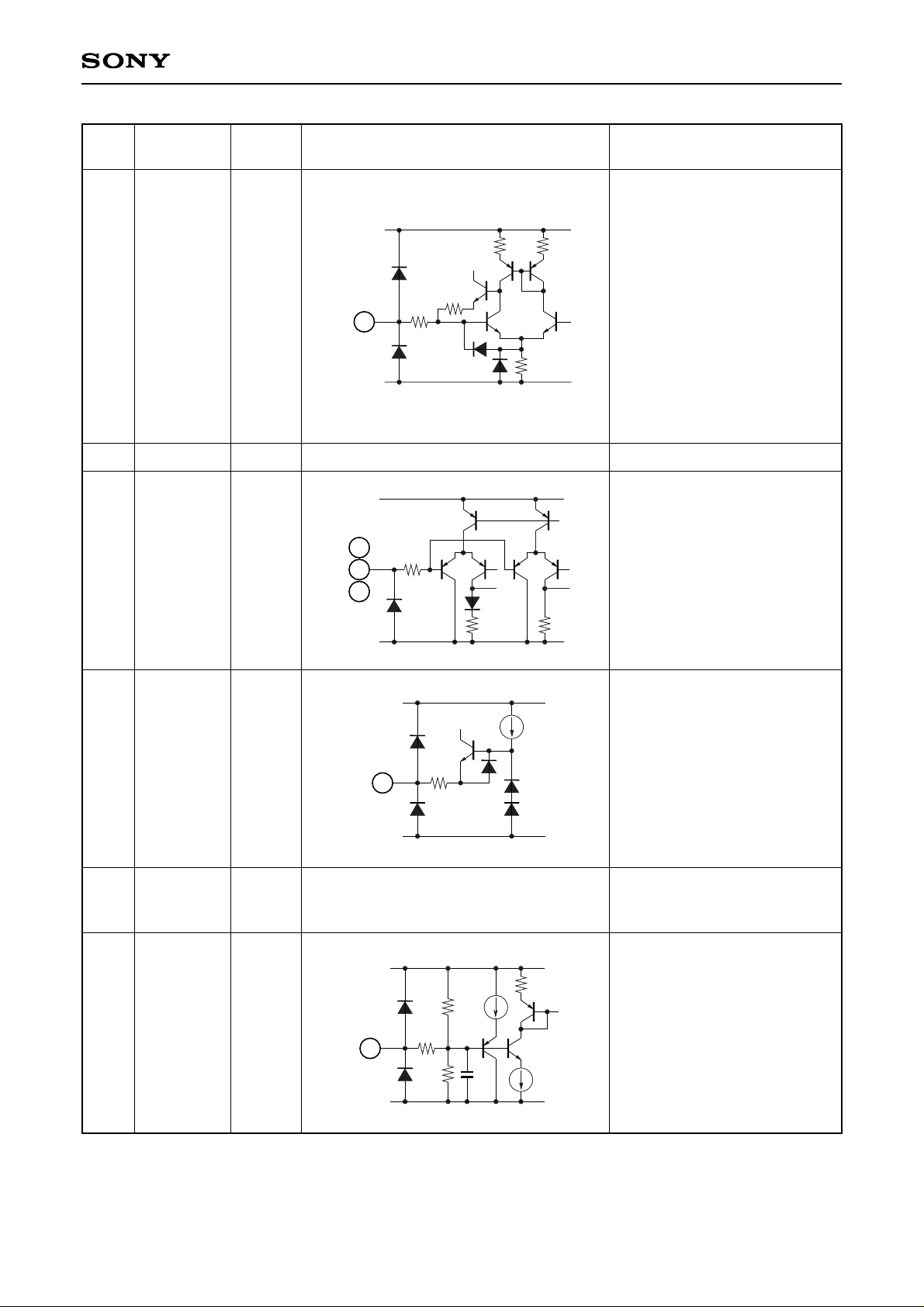
CXA3268AR
Pin
No.
8
F ADJ
Connect a resistor between this
pin and GND1 to control the
internal LPF and trap
frequencies.
Connect a 33kΩ resistor
(tolerance ±2%, temperature
characteristics ±200ppm or less).
This pin is easily affected by
external noise, so make the
connection between the pin and
external resistor, and between
the GND side of the external
resistor and the GND1 pin as
close as possible.
Analog 3.0V GND.
1.1V
—
GND1
9
Symbol
Pin
voltage
Equivalent circuit Description
VCC1
GND1
10
6.5k
8
14
15
16
SCK
SEN
SDAT
Serial clock, serial load and
serial data inputs for serial
communication.
—
VCC1
200
GND1
14
15
16
17 R INJECT
Connect a resistor for setting
the injector current of the IIL
logic circuit. Connect a 15kΩ
resistor between this pin and
GND1. Use a resistor with a
deviation of ±2% and
temperature characteristics of
±200ppm or less.
0.7V
29
GND2
Analog 12.0V GND.
(for the RGB and PSIG output
circuits)
—
VCC1
200
GND1
17
30 SIG.C
R, G, B and PSIG output DC
voltage setting.
Connect a 0.01µF capacitor
between this pin and GND1.
When using a SIG.C of other
than VCC2/2, input the SIG.C
voltage from an external
source.
Preset
VCC2/2
Variable
range:
5.0 to 6.5V
VCC2
GND1
140k
140k
200
10p
30
– 7 –
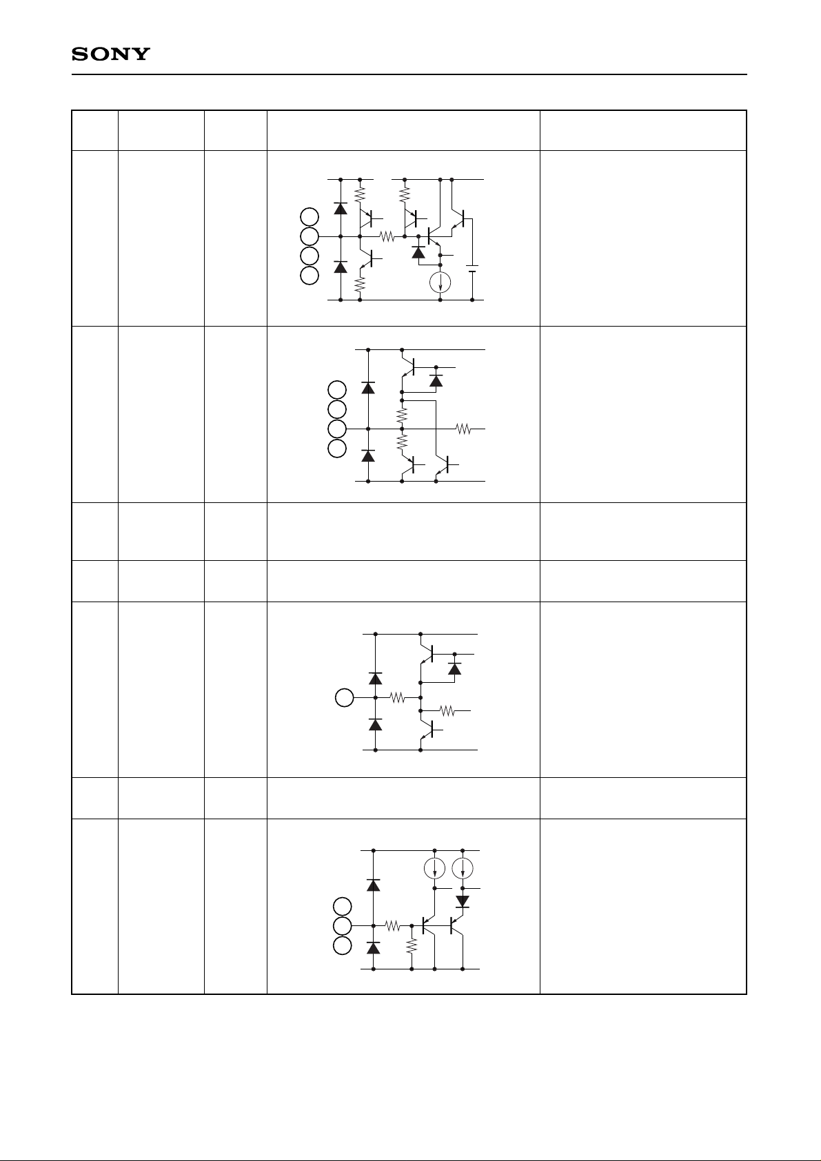
CXA3268AR
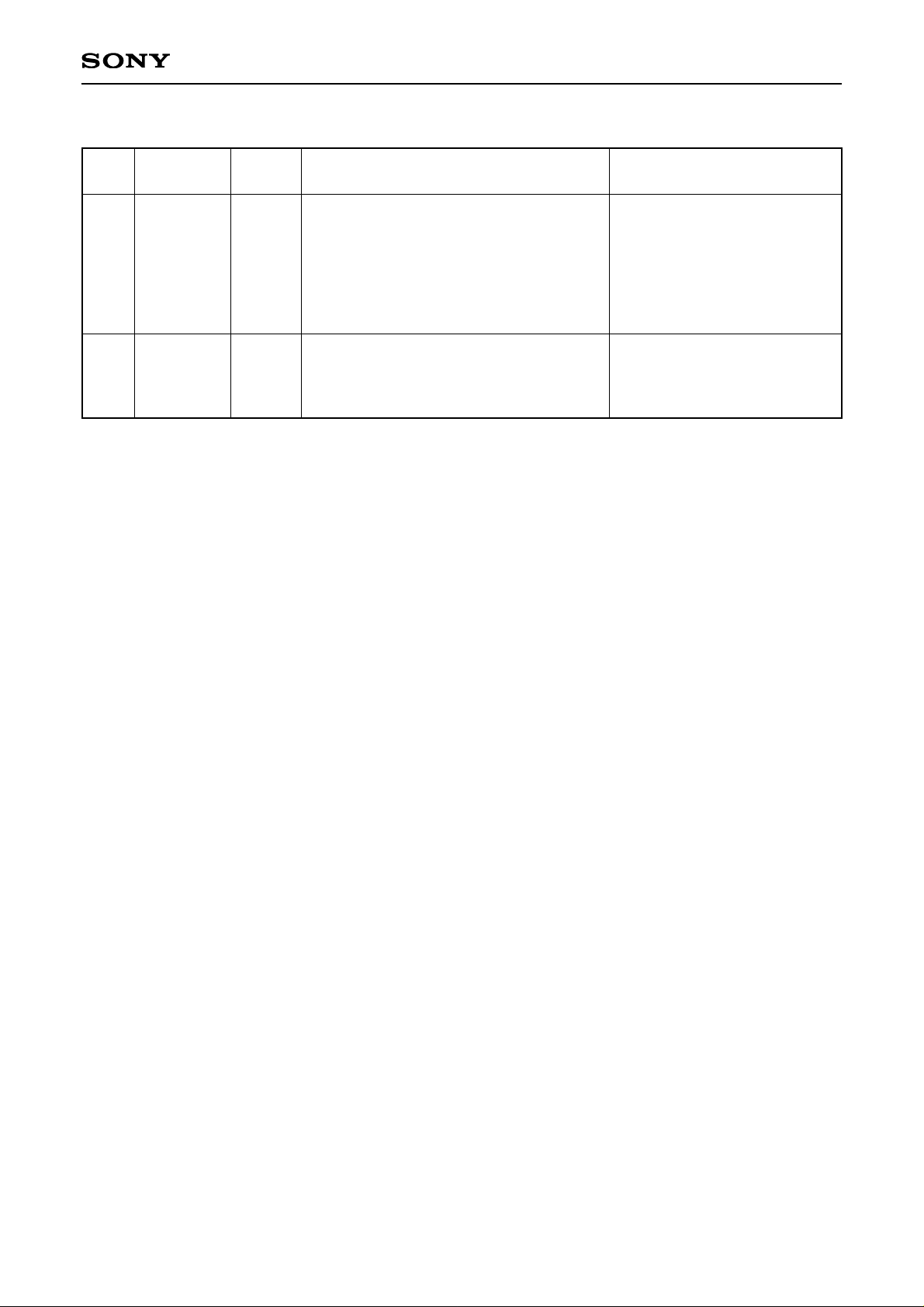
Pin
No.
31
33
35
38
B DC DET
R DC DET
G DC DET
PSIG DC DET
Smoothing capacitor connection
for the feedback circuit of R, G,
B and PSIG output DC level
control.
Connect a low-leakage
capacitor.
1.8V
Symbol
Pin
voltage
Equivalent circuit Description
VCC2 VCC1
200
GND1
31
33
35
38
32
34
36
39
B OUT
R OUT
G OUT
PSIG OUT
R, G, B and PSIG signal
outputs.
The DC level is controlled to
match the SIG.C pin voltage.
Low output in power saving
mode.
VCC2/2V output when preset.
VCC2/2
(SIG.C =
preset)
37
VCC2
Analog 12.0V power supply.
(for the RGB and PSIG output
circuits)
12.0V
41 VCC3
Analog 12.0V power supply.
(for COM (CS) output)
12.0V
VCC2
166k
10
10
GND2
32
34
36
39
42 COM
COMMON voltage output.
The output voltage is controlled
by serial communication.
—
VCC3
200
GND3
42
90k
57
58
59
OSD B
OSD R
OSD G
OSD pulse inputs.
When one of these input pins
exceeds the Vth1 level, all of
the outputs go to black limiter
level; when an input pin
exceeds the Vth2 level, only the
corresponding output goes to
white limiter level.
Vth1 =
VCC1 × 1/3
Vth2 =
VCC1 × 2/3
VCC1
50k
50k
GND1
57
59
58
43 GND3
Analog 12.0V GND.
(for COM (CS) output)
—
– 8 –
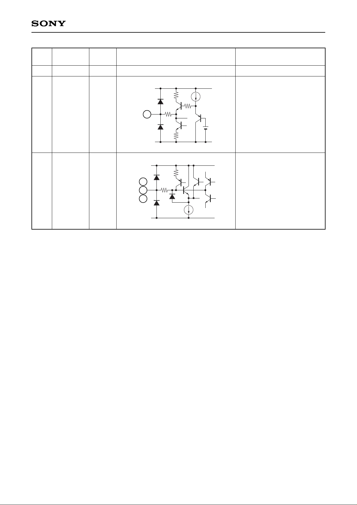
CXA3268AR
Pin
No.
69 FIL IN
H filter input.
Input the video signal via a
capacitor.
1.2V
63
VCC1
Analog 3.0V power supply.
—
Symbol
Pin
voltage
Equivalent circuit Description
VCC1
GND1
200
69
70
71
72
B/B-Y
G/Y
R/R-Y
In Y/color difference input
mode, input the Y signal to
Pin 71, the B-Y signal to Pin 70,
and the R-Y signal to Pin 72.
In RGB input mode, input the
B signal to Pin 70, the G signal
to Pin 71 and the R signal to
Pin 72.
Pedestal clamp these pins with
external coupling capacitors.
G/Y 1.8V
R/R-Y,
B/B-Y,
RGB:
1.8V
Y/color
difference:
2.0V
VDD1
GND1
200
70
71
72
– 9 –
CXA3268AR
Digital Block Pin Description
Pin
No.
1
18
23
53
54
VSS Digital 3.0V GND.—
19
20
55
VDD
Digital 3.0V power supply.—
5
14
15
16
CSYNC/HD
SCK
SEN
SDAT
Composite sync/horizontal sync
signal input, and serial clock,
serial load and serial data inputs
for serial communication.
—
10 VD
Vertical sync signal input.
—
21
22
24
CKO
CKI
RPD
Oscillation circuit output.
Oscillation circuit input.
Phase comparator output.
—
—
—
Symbol
Pin
voltage
Equivalent circuit Description
VSS
5
15
1614
VSS
10
VSS
VDD
25
VSS
VDD
67
66
68
11
64
65
26
27
45
61
62
12
25 XCLR Digital block system reset.—
11
12
26
27
45
61
62
64
65
66
67
68
DWN
WIDE
VDO
HDO
POF
HCK1
HCK2
HST
EN
VCK
VST
RGT
Digital block outputs.—
– 10 –
CXA3268AR
Test Pin Description
Pin
No.
13
40
44
49
50
51
52
TST1
TST3
TST4
TST7
TST8
TST9
TST10
Test.
Leave these pins open.
—
28
47
48
56
TST2
TST5
TST6
TST11
Test.
Connect to GND.
—
Symbol
Pin
voltage
Equivalent circuit Description
– 11 –
CXA3268AR
Setting Conditions for Measuring Electrical Characteristics
Use the Electrical Characteristics Measurement Circuit on page 22 when measuring electrical characteristics.
For measurement, the digital block must be initialized and power saving must be canceled by performing
Settings 1 and 2 below. In addition, the serial data must be set to the initial settings shown in the table below.
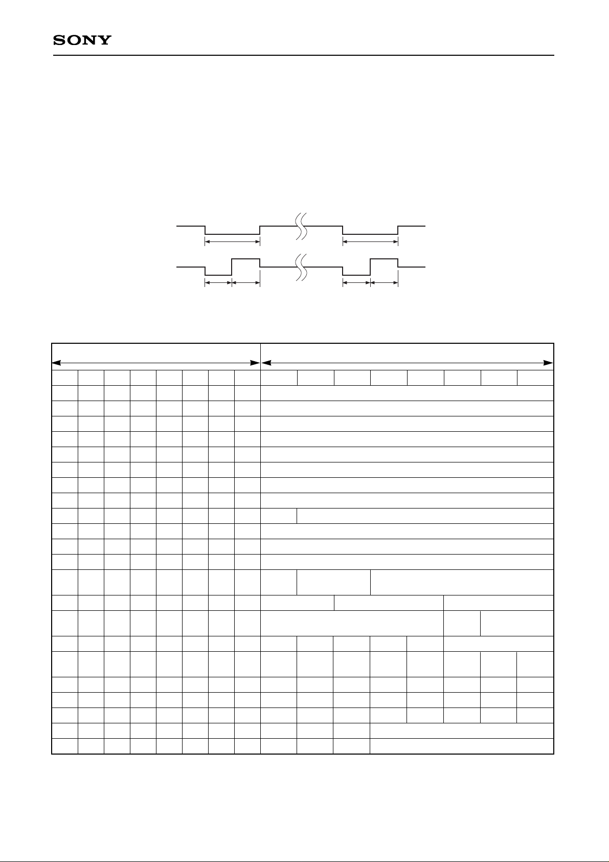
Setting 1. Horizontal AFC adjustment
Input a signal and adjust the VCO using V22 so that WL and WH of the TP24 output waveform are the same.
Setting 2. Canceling power saving mode
The power-on default is power saving mode, so clear (set all "0") serial data PS0, PS1, PS2, PS4 and SYNC GEN.
Horizontal sync
signal
RPD (Pin 24)
WS
WL WH WL WH WL = WH
WS
Fig. 1. Horizontal AFC adjustment
Serial data initial settings
Note) If there is the possibility that data may be set at other than the above-noted addresses, set these data to "0".
MSB ADDRESS LSB MSB DATA LSB
D15 D14 D13 D12 D11 D10 D9 D8 D7 D6 D5 D4 D3 D2 D1 D0
0
0
0
0
0
0
0
0
0
0
0
0
0
0
0
0
0
0
0
0
0
0
0
0
0
0
0
0
0
0
0
0
0
0
0
0
0
0
0
0
0
0
0
0
0
0
0
0
0
0
0
0
0
0
0
0
0
0
0
0
0
1
1
1
1
1
0
0
0
0
0
0
0
0
0
0
0
0
0
0
0
0
1
0
0
0
0
0
0
0
0
0
0
0
0
0
1
1
1
1
1
1
1
1
0
0
0
0
0
0
0
0
0
0
1
1
1
1
0
0
0
0
1
1
1
1
0
0
0
0
0
1
0
0
1
1
0
0
1
1
0
0
1
1
0
0
1
1
0
0
0
1
1
0
0
1
0
1
0
1
0
1
0
1
0
1
0
1
0
1
0
0
1
0
1
0
USER-BRIGHT
SUB-BRIGHT R
SUB-BRIGHT B
CONTRAST
SUB-CONTRAST R
SUB-CONTRAST B
γ-2
γ-1
0
PSIG-BRIGHT
COM-DC
COLOR
HUE
(01000110/LSB)
(10001010/LSB)
(10001010/LSB)
(00111111/LSB)
(10011111/LSB)
(10011111/LSB)
(11111111/LSB)
(11111111/LSB)
(1011111/LSB)
(10000000/LSB)
(00000000/LSB)
(10000000/LSB)
WHITE-LIMITER
(00/LSB)
BLACK-LIMITER (11111/LSB)
LPF (000/LSB)
REF (000/LSB)
FILTER (00/LSB)
PICTURE-F0
(00/LSB)
PICTURE-GAIN (00000/LSB)
0
0 0 0
MODE (1)
DA (000/LSB)
0
SLSYP (1)
0
0
0
0
0
SLEXVD (0)
SLFL (0)
0
0
0
SYNC GEN
(0)
SLDWN (0)
SLFR (0)
SLTST4 (0)
0
0
PS 4
(0)
SLRGT (0)
SL4096 (0)
SLTST3 (0)
0
SLSH2 (1)
SLCLP2 (0)
SLSH0 (1)
PS 2
(0)
SLSH1 (1)
SLCLP1 (0)
SLTST2 (0)
PS 1
(0)
SLWD (0)
SLVDP (0)
SLTST1 (0)
PS 0
(0)
SLPL (0)
SLHDP (0)
SLTST0 (0)
H-POSITION (10000)
HD-POSITION (00000)
0
0
– 12 –
CXA3268AR
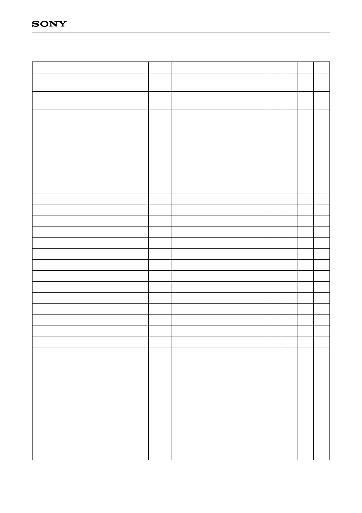
Electrical Characteristics — DC Characteristics
Analog Block Unless otherwise specified, Ta = 25°C, VCC1 = VDD =3.0V, VCC2/VCC3 = 12.0V,
SW4 = off for the current consumption measurement, see page 11 for the DAC.
Item
Current consumption 1
(Y/color difference input)
Current consumption 2
(Y/color difference input)
Current consumption 3
(Y/color difference input)
Current consumption 1 (RGB input)
Current consumption 2 (RGB input)
Current consumption 3 (RGB input)
Current consumption 1 (PS0 = 1)
Current consumption 2 (PS0 = 1)
Current consumption 3 (PS0 = 1)
Current consumption 1 (PS2 = 1)
Current consumption 1 (PS4 = 1)
Current consumption 1 (SYNC GEN = 1)
Current consumption 2 (SYNC GEN = 1)
Current consumption 3 (SYNC GEN = 1)
FIL OUT pin voltage
SYNC IN pin voltage
SYNC OUT pin voltage
F ADJ pin voltage
R INJECT pin voltage
SIG.C pin voltage
B DC DET pin voltage
R DC DET pin voltage
G DC DET pin voltage
PSIG DC DET pin voltage
FIL IN pin voltage
B/B-Y pin voltage 1
B/B-Y pin voltage 2
G/Y pin voltage
R/R-Y pin voltage 1
R/R-Y pin voltage 2
REF pin voltage (power saving mode)
OSD input resistance
I1
I2
I3
IRGB1
IRGB2
IRGB3
IPS01
IPS02
IPS03
IPS21
IPS41
ISG1
ISG2
ISG3
V2
V3
V4
V8
V17
V30
V31
V33
V35
V38
V69
V70
V70
V71
V70
V70
V7
V57
V58
V59
Measure the inflow current to Pin 63.
Measure the inflow current to Pin 37.
Measure the inflow current to Pin 41.
Measure the inflow current to Pin 63.
Measure the inflow current to Pin 37.
Measure the inflow current to Pin 41.
Measure the inflow current to Pin 63.
Measure the inflow current to Pin 37.
Measure the inflow current to Pin 41.
Measure the inflow current to Pin 63.
Measure the inflow current to Pin 63.
Measure the inflow current to Pin 63.
Measure the inflow current to Pin 37.
Measure the inflow current to Pin 41.
During no input
During no input
During no input
During Y/color difference input
During RGB input
During Y/color difference input
During RGB input
I7 = 1.5mA
1.8
1.8
0.8
0.4
5.8
1.5
1.5
1.5
1.5
0.9
1.7
1.5
1.5
1.7
1.5
80
27.0
3.8
0.90
23.0
3.8
0.90
7.5
0.18
26.5
26.5
7.0
0.18
2.1
1.1
0.2
1.1
0.7
6.0
1.8
1.8
1.8
1.8
1.2
2.0
1.8
1.8
2.0
1.8
100
37.0
5.0
1.3
30.0
5.0
1.3
10.0
0.35
1.00
36.5
36.5
9.5
0.35
1.00
2.4
1.4
0.4
1.4
1.0
6.2
2.1
2.1
2.1
2.1
1.5
2.3
2.1
2.1
2.3
2.1
0.3
120
mA
mA
mA
mA
mA
mA
mA
mA
µA
mA
mA
mA
mA
µA
V
V
V
V
V
V
V
V
V
V
V
V
V
V
V
V
V
kΩ
Symbol Measurement conditions Min. Typ. Max. Unit

– 13 –
CXA3268AR
Digital Block (including some analog block) (Ta = –15 to +75°C, VDD = VCC1 = 3.7 to 3.6V)
Item
High level input voltage
Low level input voltage
High level threshold voltage
Low level threshold voltage
Hysteresis voltage
High level threshold voltage
Low level threshold voltage
Hysteresis voltage
High level input current
Low level input current
High level input current
Low level input current
High level input current
Low level input current
High level input current
Low level input current
Low level output voltage
High level output voltage
Low level output voltage
High level output voltage
Low level output voltage
High level output voltage
Low level output voltage
High level output voltage
Output leak current
VIH
VIL
VT+1
VT–1
VT+1 – VT–1
VT+2
VT–2
VT+2 – VT–2
| IIH1 |
| IIL1 |
| IIH2 |
| IIL2 |
| IIH3 |
| IIL3 |
| IIH4 |
| IIL4 |
VOL1
VOH1
VOL2
VOH2
VOL3
VOH3
VOL4
VOH4
| IOZ |
Schmitt buffer
VI = VDD
VI = 0V
VI = VDD
VI = 0V
VI = VDD
VI = 0V
VI = VDD
VI = 0V
IOL = 1mA
IOH = –0.25mA
IOL = 2mA
IOH = –0.5mA
IOL = 4mA
IOH = –1mA
IOL = 1.5mA
IOH = –1.25mA
High impedance status
VDD × 0.7
0.6
0.4
0.6
0.2
10
10
2.6
2.6
2.6
VDD – 0.5
Symbol
Measurement
conditions
Min.
40
40
Typ.
VDD × 0.3
2.6
2.6
1.0
1.0
3.0
100
100
3.0
1.0
2.0
0.3
0.3
0.3
0.4
1.0
Max.
V
V
V
V
V
V
V
V
µA
µA
µA
µA
µA
µA
µA
µA
V
V
V
V
V
V
V
V
µA
Unit
∗1
∗2
∗3
∗4
∗5
∗6
∗7
∗8
∗9
∗10
∗11
∗12
Applicable
pins
∗1
XCLR (Pin 25), CKI (Pin 22)
∗2
CSYNC/HD (Pin 5), VD (Pin 10)
∗3
SCK (Pin 14), SEN (Pin 15), SDAT (Pin 16)
∗4
CSYNC/HD (Pin 5), CKI (Pin 22)
∗5
XCLR (Pin 25)
∗6
VD (Pin 10)
∗7
SCK (Pin 14), SEN (Pin 15), SDAT (Pin 16)
∗8
DWN (Pin 11), WIDE (Pin 12), VCK (Pin 66), VST (Pin 67), RGT (Pin 68)
∗9
RPD (Pin 24), VDO (Pin 26), HDO (Pin 27), POF (Pin 45), HST (Pin 64), EN (Pin 65)
∗10
HCK1 (Pin 61), HCK2 (Pin 62)
∗11
CKO (Pin 21). However, when measuring the output pin (CKO), the input level of the input pin (CKI) should
be 0V or VDD.
∗12
RPD (Pin 24)
 Loading...