

Sony CXA3250AN Datasheet

—1—
E99866-TE
Sony reserves the right to change products and specifications without prior notice. This information does not convey any license by
any implication or otherwise under any patents or other right. Application circuits shown, if any, are typical examples illustrating the
operation of the devices. Sony cannot assume responsibility for any problems arising out of the use of these circuits.
Absolute Maximum Ratings (Ta=25 °C)
• Supply voltage VCC1, VCC2 –0.3 to +5.5 V
VCC3 –0.3 to +10.0 V
• Storage temperature Tstg –55 to +150 °C
• Allowable power dissipation
PD 580 mW
(when mounted on a printed circuit board)
Operating Conditions
• Supply voltage VCC1, VCC2 4.75 to 5.30 V
VCC3 4.75 to 9.45 V
• Operating temperature Topr –25 to +75 °C
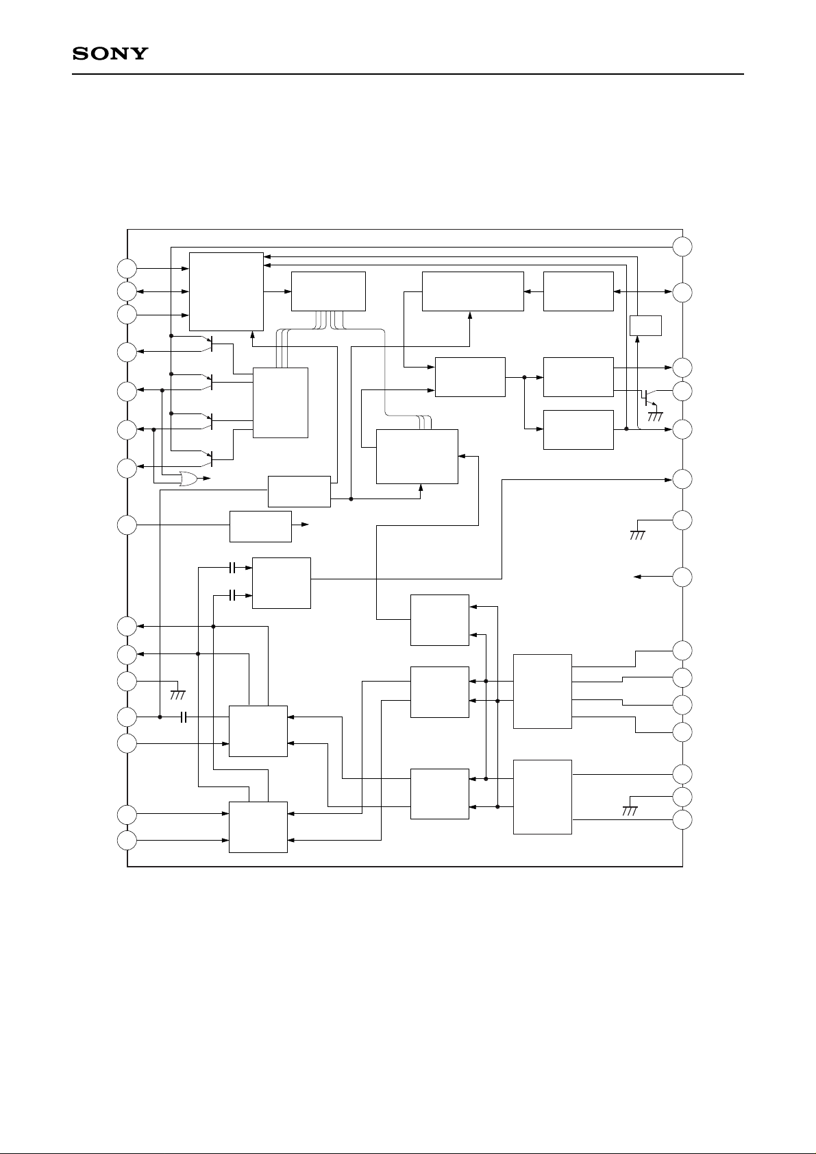
Description
The CXA3250AN is a monolithic TV tuner IC which
integrates local oscillator and mixer circuits for VHF
band, local oscillator and mixer circuits for UHF
band, an IF amplifier and a tuning PLL onto a single
chip, enabling further miniaturization of the tuner.
Features
• Superior cross modulation
• Balanced UHF oscillator (4 pins) with excellent
oscillation stability
• Supports both I2C and 3-wire bus modes
• Automatic identification of 18, 19 or 27-bit control
(during 3-wire bus mode)
• On-chip A/D converter (during I2C bus mode)
• On-chip high voltage drive transistor for charge
pump
• Reference frequency selectable from 31.25, 50 or
62.5 kHz (when using a 4 MHz crystal)
• Low-phase noise synthesizer
• On-chip 4-output band switch (supports output
voltages from 5 to 9 V)
Applications
• TV tuners
• VCR tuners
• CATV tuners
Structure
Bipolar silicon monolithic IC
All Band TV Tuner IC with On-chip PLL
30 pin SSOP (Plastic)
CXA3250AN
This IC has the pins whose electrostatic discharge strength is weak as the operating frequency is high and the high-frequency
process is used for this IC.
Take care of handling the IC.
For the availability of this product, please contact the sales office.
—2—
CXA3250AN
Block Diagram and Pin Configuration
Shift
Register
Programable
Divider
14/15bit
Divider
1/64, 80, 128
BUS
Interface
REF
OSC
Charge
Pump
LOCK
Det
IF AMP
Buffer
VHF
MIX
Mode
Select
V.REG
Band
SW
Driver
UHF
OSC
VHF
OSC
Bias
Phase
Detector
ADC
VHF
MIX
Buffer
Buffer
UHF
MIX
VSW
23
24
25
26
28
29
30
27
19
20
21
22
16
17
18
1
2
3
4
5
6
7
8
9
10
11
12
13
14
15
CL
DA
ADSW
/CE
BS3
BS1
BS2
BS4
V
CC1
MIXout1
MIXout2
GND1
BYP/MS
VHFin
UHFin1
UHFin2
V
CC3
REFOSC
CPO
VT
LOCK
/ADC
IFOUT
GND2
VCC2
UOSCB2
UOSCE2
UOSCE1
UOSCB1
VOSC2
GND
VOSC1
—3—
CXA3250AN
Pin Description
Pin No.
1
2
3
4
5
6
7
8
9
10
11
12
13
14
15
16
17
18
19
20
21
22
23
24
25
26
27
28
29
30
Symbol
CL
DA
CE/ADSW
BS3
BS1
BS2
BS4
VCC1
MIXOUT1
MIXOU2
GND1
BYP/MS
VHFIN
UHFIN1
UHFIN2
VOSC1
GND
VOSC2
UOSCB1
UOSCE1
UOSCE2
UOSCB2
VCC2
GND2
IFOUT
LOCK/ADC
VT
CPO
REFOSC
VCC3
Description
CLOCK/SCL (I2C bus)
DATA/SDA (I2C bus)
Enable/address selection (I2C bus)
Band switch output 3
Band switch output 1
Band switch output 2
Band switch output 4
Analog circuit VCC
MIX output
MIX output
Analog circuit GND
VHF input GND and control bus switching
VHF input
UHF input
UHF input
VHF oscillator (base input)
GND
VHF oscillator (collector output)
UHF oscillator (base pin)
UHF oscillator (emitter pin)
UHF oscillator (emitter pin)
UHF oscillator (base pin)
PLL circuit VCC
PLL circuit GND
IF output
LOCK signal output/ADC input (I2C bus)
VC drive voltage output (open collector)
Charge pump output (loop filter connection)
Crystal connection
Band switch power supply
—4—
CXA3250AN
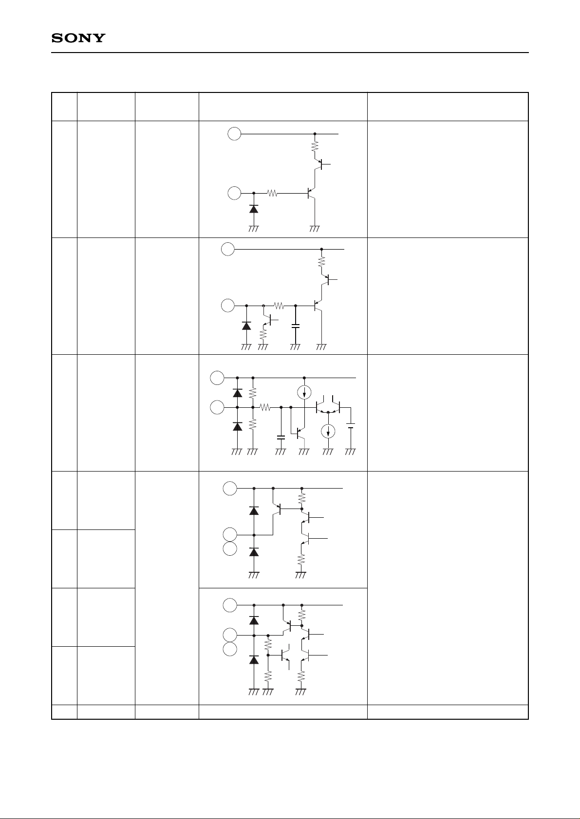
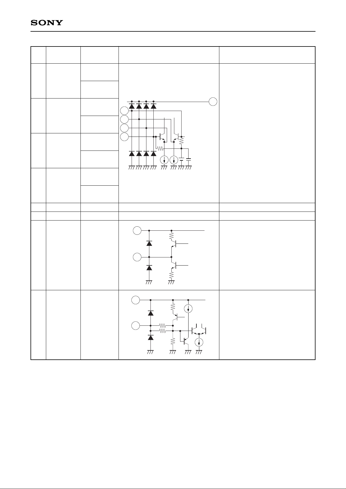
Pin Description and Equivalent Circuit
Pin
Symbol
Pin voltage
Equivalent circuit Description
No. [V]
1
2
3
4
7
5
6
8
CL
DA
ADSW/CE
BS3
BS4
BS1
BS2
VCC1
—
—
1.25
(when open)
ON : 4.8
OFF : 0.0
—
40k
1
23
40k
2.5p
2
23
20
150k
50k
5p
3
23
7
30
4
6
30
5
25k
12k
Clock input.
Data input.
I2C bus setting :
Address selection.
Bits 1 and 2 of the address byte
are controlled.
3-wire bus setting :
Enable input.
Band switch outputs.
The pin corresponding to the
selected band goes High.
Analog circuit power supply.—
—5—
CXA3250AN
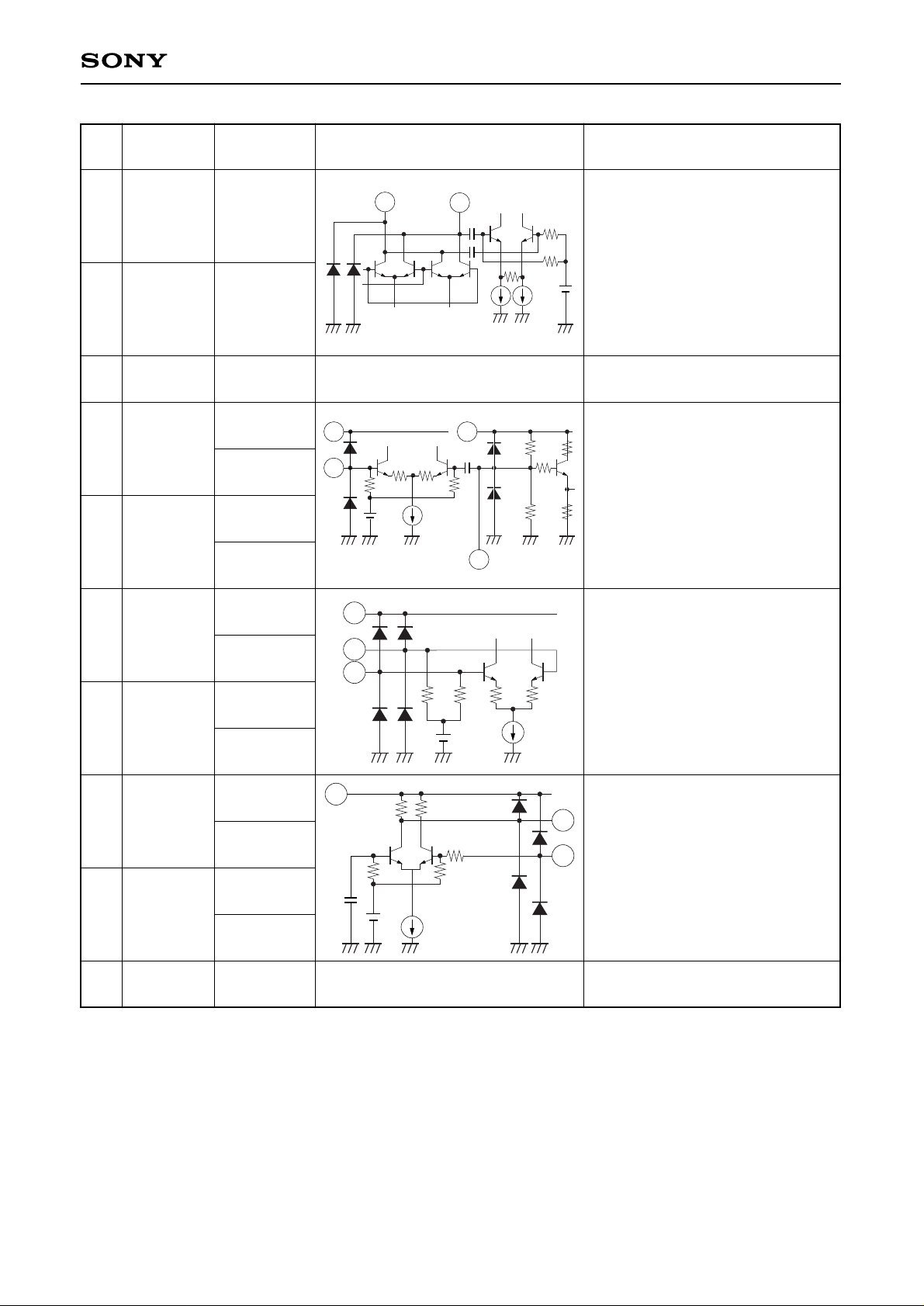
Pin
Symbol
Pin voltage
Equivalent circuit Description
No. [V]
9
10
11
12
13
14
15
16
18
17
MIXOUT1
MIXOUT2
GND1
BYP/MS
VHFin
UHFin1
UHFin2
VOSC1
VOSC2
GND
—
—
—
3.8 during
VHF reception
3.8 during
UHF reception
2.6 during
VHF reception
0.1 during
UHF reception
2.6 during
UHF reception
0.1 during
VHF reception
2.6 during
UHF reception
0.1 during
VHF reception
2.1 during
VHF reception
2.3 during
UHF reception
4.2 during
VHF reception
5.0 during
UHF reception
—
9
10
24k
15p
3k 3k
76k
8
12
13
23
3k 3k
8
14
15
3k 3k
50
400
8
16
18
Mixer output.
These pins output the signal with
open collector, and they must be
connected to the power supply via
the load.
Analog circuit GND.
Pin 12 : VHF input grounding and
control bus switching.
Pin 13 : VHF input.
Input format is the
unbalanced input.
UHF inputs.
Input the signal to Pins 14 and 15
symmetrically or ground either of
Pin 14 or 15 with the capacitor and
input the signal to the rest.
External resonance circuit
connection for VHF oscillator.
GND for separating the analog and
PLL systems.
—
—
—6—
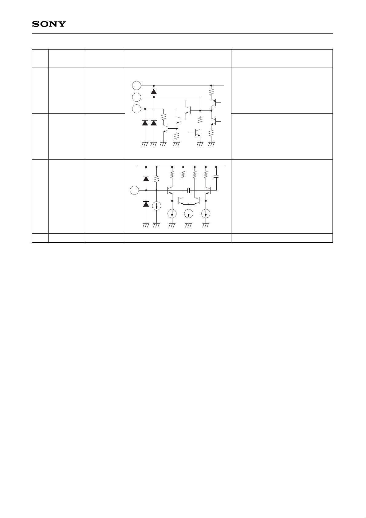
CXA3250AN
Pin
Symbol
Pin voltage
Equivalent circuit Description
No. [V]
19
20
21
22
23
24
25
26
UOSCB1
UOSCE1
UOSCE2
UOSCB2
VCC2
GND2
IFOUT
LOCK/ADC
2.1 during
UHF reception
2.3 during
VHF reception
1.4 during
UHF reception
1.8 during
VHF reception
1.4 during
UHF reception
1.8 during
VHF reception
2.1 during
UHF reception
2.3 during
VHF reception
—
—
2.7
—
3k
3k
8
19
20
21
22
8
25
250
5k
500k
23
26
External resonance circuit
connection for UHF oscillator.
PLL circuit power supply.
PLL circuit GND.
IF output.
I2C bus setting :
5-level A/D converter input.
3-wire bus setting :
Lock detection.
Low when locked, High when
unlocked.
—
—
—7—
CXA3250AN
Pin
Symbol
Pin voltage
Equivalent circuit Description
No. [V]
27
28
29
30
VT
CPO
REFOSC
VCC3
—
2.0
4.3
—
70
23
27
28
60k
30p
30p
29
Varicap drive voltage output.
This pin outputs the signal with
open collector, and this must be
connected to the tuning power
supply via the load.
Charge pump output.
Connects the loop filter.
Crystal connection for reference
oscillator.
Power supply for external supply.—
—8—
CXA3250AN
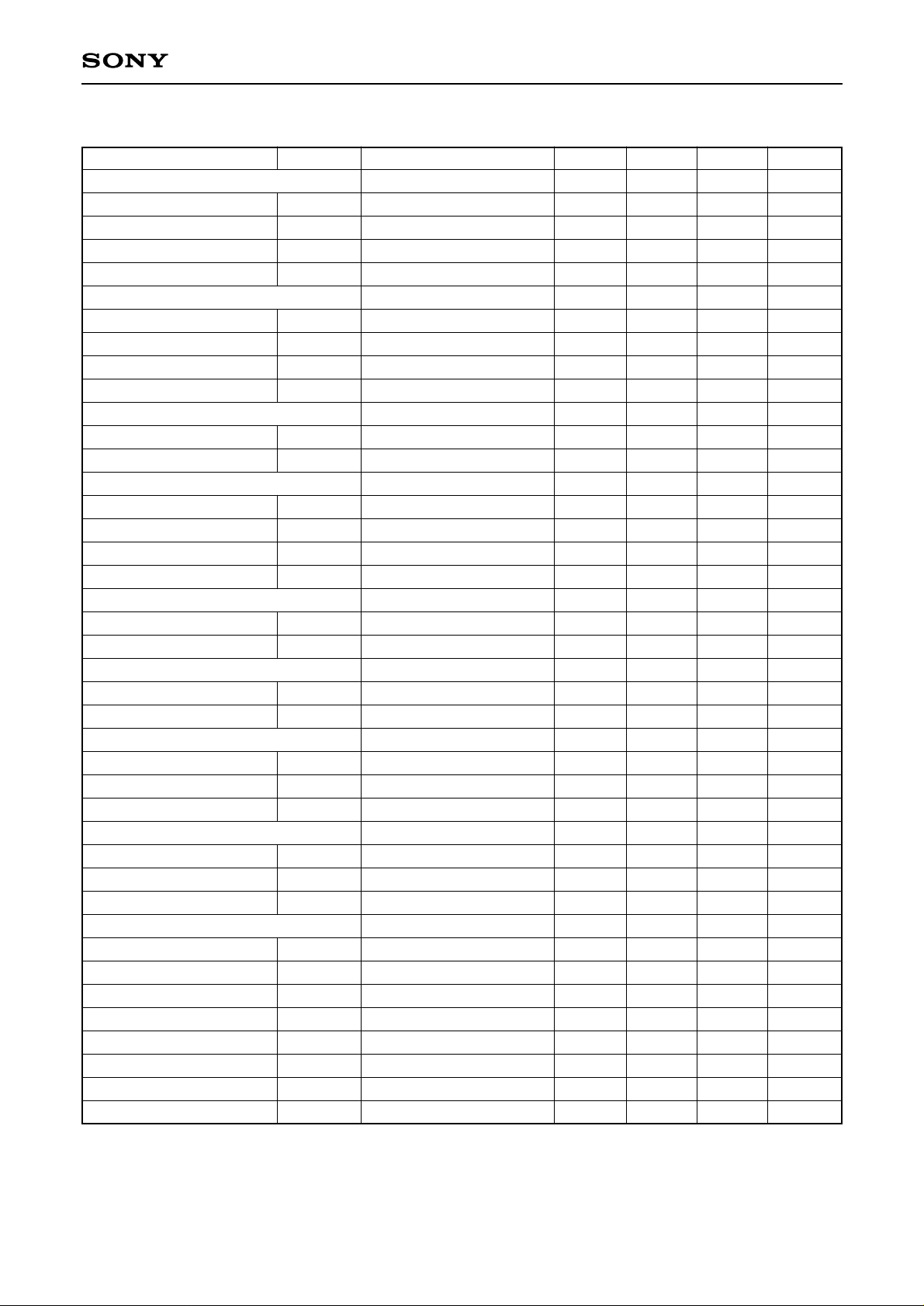
Electrical Characteristics
Circuit Current (VCC=5 V, Ta=25 °C)
Item
Circuit current A
Circuit current D
Symbol
AICCV
AICCU
DICC
Measurement conditions
VCC1 current, band switch output
open during VHF operation
VCC1 current, band switch output
open during UHF operation
VCC2 current
Min. Typ. Max. Unit
38 52 70 mA
39 53 71 mA
10 16 22 mA
Item
Conversion gain
Noise figure
∗1, ∗2
1 % cross
∗1, ∗3
modulation
Maximum output
power
Switch ON drift
∗4
Symbol
CG1
CG2
CG3
CG4
NF1
NF2
NF3
NF4
CM1
CM2
CM3
CM4
Pomax
∆ fsw1
∆ fsw2
∆ fsw3
∆ fsw4
Measurement conditions
VHF operation fRF=55 MHz
VHF operation fRF=360 MHz
UHF operation fRF=360 MHz
UHF operation fRF=800 MHz
VHF operation fRF=55 MHz
VHF operation fRF=360 MHz
UHF operation fRF=360 MHz
UHF operation fRF=800 MHz
VHF operation
fD=55 MHz, fUD=±12 MHz
VHF operation
fD=360 MHz, fUD=±12 MHz
UHF operation
fD=360 MHz, fUD=±12 MHz
UHF operation
fD=800 MHz, fUD=±12 MHz
50 Ω load saturation output
VHF operation fOSC=100 MHz
∆ f from 3 s to 3 min after switch ON
VHF operation fOSC=405 MHz
∆ f from 3 s to 3 min after switch ON
UHF operation fOSC=405 MHz
∆ f from 3 s to 3 min after switch ON
UHF operation fOSC=845 MHz
∆ f from 3 s to 3 min after switch ON
Min. Typ. Max. Unit
18 21 24 dB
19 22 25 dB
22.5 25.5 28.5 dB
24 27 30 dB
12 15 dB
11 14 dB
10 13 dB
11 14 dB
100 104 dBµ
99 103 dBµ
96 100 dBµ
90 94 dBµ
+8 +11 dBm
±300 kHz
±600 kHz
±350 kHz
±350 kHz
OSC/MIX/IF Amplifier Block
—9—
CXA3250AN
Item
Supply voltage ∗4
drift
Oscillator phase
noise
Reference leak
Lock-up time
Symbol
∆ fst1
∆ fst2
∆ fst3
∆ fst4
C/N V
C/N U
REFL
LUT 1
LUT 2
Measurement conditions
VHF operation fOSC=100 MHz
∆ f when VCC 5 V changes ±5 %
VHF operation fOSC=405 MHz
∆f when VCC 5 V changes ±5 %
UHF operation fOSC=405 MHz
∆ f when VCC 5 V changes ±5 %
UHF operation fOSC=845 MHz
∆f when VCC 5 V changes ±5 %
10 kHz offset
10 kHz offset
Phase comparison frequency of
62.5 kHz, CP : 1
VHF operation fOSC=95 MHz ⇔
fOSC=395 MHz CP : 1
UHF operation fOSC=413 MHz ⇔
fOSC=847 MHz CP : 1
Min. Typ. Max. Unit
±200 kHz
±250 kHz
±150 kHz
±150 kHz
82
dBc/Hz
78
55 dB
24 70
ms
36 70
∗1 Value measured with untuned input.
∗2 NF meter direct-reading value (DSB measurement).
∗3 Value with a desired reception signal input level of –30 dBm, an interference signal of 100 kHz/30 % AM,
and an interference signal level where S/I=46 dB measured with a spectrum analyzer.
∗4 Value when the PLL is not operating.
—10—
CXA3250AN
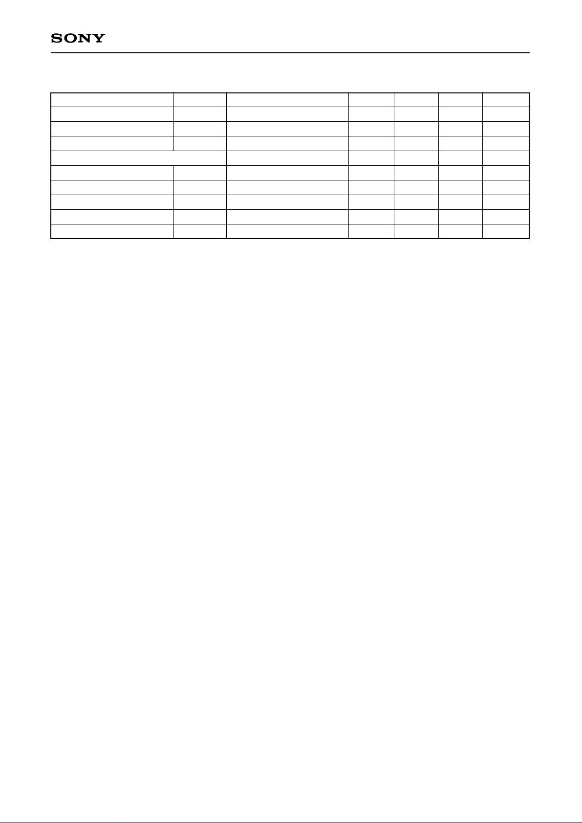
Item
CL, DA and CE pins
“H” level input voltage
“L” level input voltage
“H” level input current
“L” level input current
CE input
“H” level input voltage
“L” level input voltage
“H” level input current
“L” level input current
SDA output
“H” output leak current
“L” output voltage
CPO (charge pump)
Output current 1
Leak current 1
Output current 2
Leak current 2
VT (VC voltage output)
Maximum output voltage
Minimum output voltage
LOCK
“H” output voltage
“L” output voltage
REFOSC
Oscillation frequency range
Input capacitance
Negative resistance
Band SW
Output current
Saturation voltage
Leak current
Bus timing (I2C bus)
SCL clock frequency
Start waiting time
Start hold time
“L” hold time
“H” hold time
Start setup time
Data hold time
Data setup time
Symbol
VIH
VIL
IIH
IIL
VIH
VIL
IIH
IIL
ISDALK
VSDAL
ICPO1
LeakCP1
ICPO2
LeakCP2
VTH
VTL
VLOCKH
VLOCKL
FXTOSC
CXTOSC
RNEG
IBS
VSAT
LeakBS
fSCL
tWSTA
tHSTA
tLOW
tHIGH
tSSTA
tHDAT
tSDAT
Measurement conditions
VIH=VCC
VIL=GND
VIH=VCC
VIL=GND
Vin=5.5 V
Iout=–3 mA
Byte4/bit6=0
Byte4/bit6=0
Byte4/bit6=1
Byte4/bit6=1
When locked
When unlocked
Crystal source impedance
When ON
When ON Source current=20 mA
When OFF
Min. Typ. Max. Unit
3 VCC V
GND 1.5 V
0 –0.1 µA
–0.3 –4 µA
3 VCC V
GND 1.5 V
–100 –200 µA
35 100 µA
5 µA
GND 0.4 V
±35 ±50 ±75 µA
30 nA
±140 ±200 ±300 µA
100 nA
33 V
0.5 0.8 V
VCC–0.5 VCC V
0 0.5 V
3 12 MHz
22 24 26 pF
–2.0 –1.0 kΩ
–25 mA
120 240 mV
0.5 3 µA
0 400 kHz
1300 ns
600 ns
1300 ns
600 ns
600 ns
0 900 ns
600 ns
PLL Block
—11—
CXA3250AN
Item
Rise time
Fall time
Stop setup time
Bus timing (3-wire bus)
Data setup time
Data hold time
Enable waiting time
Enable setup time
Enable hold time
Symbol
tR
tF
tSSTO
tSD
tHD
tWE
tSE
tHE
Measurement conditions Min. Typ. Max. Unit
300 ns
300 ns
600 ns
300 ns
600 ns
300 ns
300 ns
600 ns
PLL Block
 Loading...