

Sony CXA3246Q Datasheet

CXA3246Q
8-bit 120MSPS Flash A/D Converter
Description
The CXA3246Q is an 8-bit high-speed flash A/D
converter capable of digitizing analog signals at the
maximum rate of 120MSPS. ECL, PECL or TTL can
be selected as the digital input level in accordance
with the application. The TTL digital output level
allows 1:2 demultiplexed output.
Features
• Differential linearity error: ±0.5LSB or less
• Integral linearity error: ±0.5LSB or less
• High-speed operation with a maximum conversion
rate of 120MSPS
• Low input capacitance: 10pF
• Wide analog input bandwidth: 250MHz
• Low power consumption: 500mW
• 1:2 demultiplexed output
• 1/2 frequency-divided clock output
(with reset function)
• Compatible with ECL, PECL and TTL digital input
levels
• TTL output "H" levels: 2.8V (Typ.)
• +3.3V line CMOS IC direct connecting available
• Single +5V power supply operation available
• Surface mounting package (48-pin QFP)
Pin Configuration (Top View)
Structure
Bipolar silicon monolithic IC
Applications
• Magnetic recording (PRML)
• Communications (QPSK, QAM)
• LCDs
• Digital oscilloscopes
– 1 –
E97902A8X-PS
Sony reserves the right to change products and specifications without prior notice. This information does not convey any license by
any implication or otherwise under any patents or other right. Application circuits shown, if any, are typical examples illustrating the
operation of the devices. Sony cannot assume responsibility for any problems arising out of the use of these circuits.
CLK/E
N.C.
CLK/T
N.C.
N.C.
DV
CC2
DGND2
PAD0
PAD1
PAD2
PAD3
CLKN/E
PAD4
PAD7
PAD6
DGND1
DV
CC
1
DV
CC
2
DGND2
PBD0
PBD1
PBD2
PBD3
PAD5
RESETN/E
SELECT
RESETN/T
INV
CLKOUT
DV
CC2
DGND2
PBD7
PBD6
PBD5
PBD4
RESET/E
DV
EE
3
V
RM
1
AGND
AV
CC
V
IN
V
RM
2
AV
CC
V
RM
3
AGND
V
RT
DGND3
V
RB
13
14
15
16
17
18
19
20
21
22
23
24
25
26
27
28
29
30
40
39
38
37
36
35
34
31
32
33
41
42
43
44
45
46
47
48
2
3
4
5
6
7
8
9
10
11
12 1
48 pin QFP (Plastic)
LEAD TREATMENT: PALLADIUM PLATING
– 2 –
CXA3246Q
Absolute Maximum Ratings (Ta = 25°C)
Unit
• Supply voltage AVCC, DVCC1, DVCC2 –0.5 to +7.0 V
DGND3 –0.5 to +7.0 V
DVEE3 –7.0 to +0.5 V
DGND3 – DVEE3 –0.5 to +7.0 V
• Analog input voltage VIN VRT – 2.7 to AVCC V
• Reference input voltage VRT 2.7 to AVCC V
VRB VIN – 2.7 to AVCC V
|VRT – VRB| 2.5 V
• Digital input voltage ECL/PECL input pin DVEE3 – 0.5 to DGND3 + 0.5 V
TTL input pin DGND1 – 0.5 to DVCC1 + 0.5 V
VID
∗
1
(|
∗∗∗
/E –
∗∗∗
N/E|) 2.7 V
• Storage temperature Tstg –65 to +150 °C
• Allowable power dissipation PD 1.6 W
(when mounted on a two-layer glass fabric base epoxy board with dimentions of 50mm × 50mm, 1.6mm thick)
Recommended Operating Conditions
With a single power supply With dual power supply Unit
Min. Typ. Max. Min. Typ. Max.
• Supply voltage DVCC1, DVCC2, AVCC +4.75 +5.0 +5.25 +4.75 +5.0 +5.25 V
DGND1, DGND2, AGND –0.05 0 +0.05 –0.05 0 +0.05 V
DGND3 +4.75 +5.0 +5.25 –0.05 0 +0.05 V
DVEE3 –0.05 0 +0.05 –5.5 –5.0 –4.75 V
• Analog input voltage VIN VRB VRT VRB VRT V
•
Reference input voltage
VRT +2.9 +4.1 +2.9 +4.1 V
VRB +1.4 +2.6 +1.4 +2.6 V
|VRT – VRB| 1.5 2.1 1.5 2.1 V
• Digital input voltage
ECL/PECL input pin
: VIH
DVEE3 + 1.5 DGND3 DVEE3 + 1.5 DGND3
V
: VIL
DVEE3 + 1.1 VIH – 0.4 DVEE3 + 1.1 VIH – 0.4
V
TTL input pin : VIH 2.0 2.0 V
: VIL 0.8 0.8 V
VID
∗
1
(|
∗∗∗
/E –
∗∗∗
N/E|) 0.4 0.8 0.4 0.8 V
•
Maximum conversion rate
Fc (Straight mode) 100 100 MSPS
(DMUX mode) 120 120 MSPS
• Ambient temperature Ta –20 +75 –20 +75 °C
∗
1
VID: Input Voltage Differential
ECL and PECL switching level
VID
V
IL (min.)
V
IH
VTH (DGND3 – 1.2V)
V
IL
VIH (max.)
DGND3

– 3 –
CXA3246Q
Pin Description
[Symbol] [Pin No.] [Description]
Digital power supply
Bottom reference voltage
Analog ground
Reference voltage mid point
Analog power supply
Analog signal input
Reference voltage mid point
Analog power supply
Reference voltage mid point
Analog ground
Reference voltage (typ.)
Digital power supply
ECL/PECL clock input
ECL/PECL clock input
TTL clock input
No connected pin
Digital power supply
Digital ground
PA side data output
Digital ground
Digital power supply
Digital power supply
Digital ground
PB side data output
Digital ground
Digital power supply
Clock output
Data output polarity inversion
Output mode selection
TTL reset input
ECL/PECL reset input
ECL/PECL reset input
1
2
3
4
5
6
7
8
9
10
11
12
13
14
15
16 to 18
19
20
21 to 28
29
30
31
32
33 to 40
41
42
43
44
45
46
47
48
DVEE3
VRB
AGND
VRM1
AVCC
VIN
VRM2
AVCC
VRM3
AGND
VRT
DGND3
CLK/E
CLKN/E
CLK/T
N.C.
DVCC2
DGND2
PAD0 to PAD7
DGND1
DVCC1
DVCC2
DGND2
PBD0 to PBD7
DGND2
DVCC2
CLKOUT
INV
SELECT
RESETN/T
RESET/E
RESETN/E
0V
1.4 to 2.6V
0V
—
+5V
VRB to VRT
—
+5V
—
0V
2.9 to 4.1V
+5V
PECL
PECL
TTL
—
+5V
0V
TTL
0V
+5V
+5V
0V
TTL
0V
+5V
TTL
TTL
TTL
TTL
PECL
PECL
–5.0V
1.4 to 2.6V
0V
—
+5V
VRB to VRT
—
+5V
—
0V
2.9 to 4.1V
0V
ECL
ECL
TTL
—
+5V
0V
TTL
0V
+5V
+5V
0V
TTL
0V
+5V
TTL
TTL
TTL
TTL
ECL
ECL
Typical voltage
level with a single
power supply
Typical voltage
level with dual
power supply
– 4 –
CXA3246Q
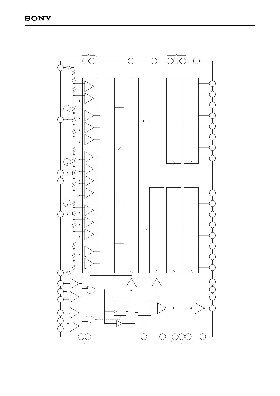
Block Diagram
6bit
VRT
2
3
5
8
10
12
13
14
16
17
18
19
20
21
22
23
24
25
26
27
28
29
30
40
39
38
37
36
35
34
31
32
33
41
42
44
1
1
2
r/2
63
64
•
•
•
65
126
127
•
•
•
128
129
191
192
•
•
•
193
254
255
•
•
•
r
6bit
9
7
4
r1
r2
r
r
r
r
r
r
r
r
r
r
r
r
r
r
/2
6bit
6bit
8bit
8bit
15
46
47
48
Select
D Q
Q
45
SELECT
11
43
DGND1 DVEE3
DGND2
AGND
AVCC DVCC2
DV
CC1INV DGND3
VRM3
VIN
VRM2
6
V
RB
VRM1
CLK/T
CLK/E
CLKN/E
RESETN/T
RESETN/E
RESET/E
CLKOUT
PAD0
PAD1
PAD2
PAD3
PAD4
PAD5
PAD6
PAD7
PBD0
PBD1
PBD2
PBD3
PBD4
PBD5
PBD6
PBD7
TTLOUT
LATCH A
TTLOUT
LATCH B
6bit LATCH + ENCODER
ENCODER
(LSB)
(MSB)
(LSB)
(MSB)
LATCH B
N.C.
N.C.
N.C.
– 5 –
CXA3246Q
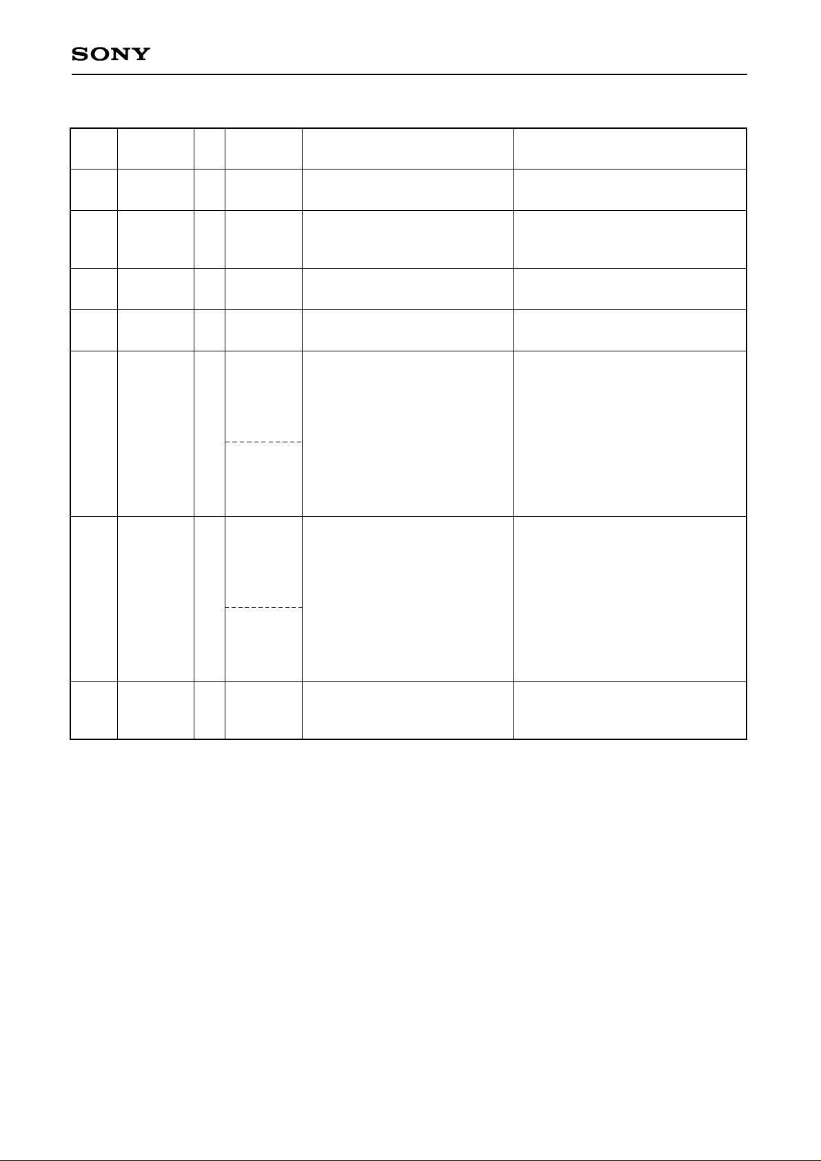
Pin Description and I/O Pin Equivalent Circuit
Analog ground.
Separated from the digital ground.
Analog power supply.
Separated from the digital power
supply.
Digital ground.
Digital power supply.
Digital power supply.
Ground for ECL input.
+5V for PECL and TTL inputs.
Digital power supply.
–5V for ECL input.
Ground for PECL and TTL inputs.
No connected pin.
Not connected with the internal
circuits.
N.C.
16, 17
18
3, 10
5, 8
20, 29
32, 41
19, 30
31, 42
12
1
AGND
AVCC
DGND1
DGND2
DVCC1
DVCC2
DGND3
DVEE3
GND
+5V
(typ.)
GND
+5V
(typ.)
+5V (typ.)
(With a
single
power
supply)
GND
(With dual
power
supply)
GND
(With a
single
power
supply)
–5V (typ.)
(With dual
power
supply)
Pin
No.
Symbol I/O
Standard
voltage level
Equivalent circuit Description

– 6 –
CXA3246Q
Pin
No.
15 CLK/T
Clock input.
46
RESETN/T
TTL
TTL
Vcc
or
GND
Reset signal input.
When left open, this pin goes to high
level. When set to low level, the
built-in CLK frequency divider circuit
can be reset.
44 INV
Data output polarity inversion input.
When left open, this input goes to
high level.
(See Table 1. I/O Correspondence
Table.)
45
SELECT
Data output mode selection.
(See Table 2. Operation Mode
Table.)
Symbol
Standard
voltage level
Equivalent circuit Description
15
46
DVCC1
DGND1
DVEE3
44
45
or
,
1.5V
I
I
I
I/O
Clock input.
CLK/E complementary input.
When left open, this pin goes to the
threshold voltage.
Only CLK/E can be used for
operation, but complementary inputs
are recommended to attain fast and
stable operation.
Reset signal input.
When set to low level, the built-in
CLK frequency divider circuit can be
reset.
RESETN/E complementary input.
When left open, this pin goes to the
threshold voltage. Only RESETN/E
can be used for operation.
ECL/
PECL
13
14
48
47
CLK/E
CLKN/E
RESETN/E
RESET/E
I
I
I
I
13
14
48
47
DGND3
DV
EE3

– 7 –
CXA3246Q
4.0V
(typ.)
11
VRT
Top reference voltage.
By-pass to AGND with a 1µF tantal
capacitor and a 0.1µF chip capacitor.
VRB +
(VRT – VRB)
9
VRM3
Reference voltage mid point.
By-pass to AGND with a 0.1µF chip
capacitor.
7
VRM2
Reference voltage mid point.
By-pass to AGND with a 0.1µF chip
capacitor.
4
VRM1
Reference voltage mid point.
By-pass to AGND with a 0.1µF chip
capacitor.
2.0V
(typ.)
2
VRB
Bottom reference voltage.
By-pass to AGND with a 1µF tantal
capacitor and a 0.1µF chip capacitor.
r1
r/2
Comparator 1
Comparator 63
Comparator 64
Comparator 128
Comparator 191
Comparator 127
Comparator 192
Comparator 255
r
r
2
r/2
r
r
r
r
4
7
9
2
11
r
I
I
4
3
4
2
VRB +
(VRT – VRB)
4
1
VRB +
(VRT – VRB)
Pin
No.
Symbol I/O
Standard
voltage level
Equivalent circuit Description
Clock output.
(See Table 2. Operation Mode Table.)
TTL output; the high level is
clamped to approximately 2.8V.
21
to
28
PAD0
to
PAD7
Port A side data output.
TTL output; the high level is
clamped to approximately 2.8V.
33
to
40
PBD0
to
PBD7
43 CLKOUT
Port B side data output.
TTL output; the high level is
clamped to approximately 2.8V.
6 VIN
VRT
to
VRB
I
TTL
O
O
O
Analog input.
AVCC
Comparator
Vref
AGND
DVEE3
AVCC
6
DVCC2
DGND2
DVCC1
DGND1
100k
DVEE3
21
28
33
40
43
to
to
 Loading...