

Sony CXA3222N Datasheet

TX Gain Control Amplifier
For the availability of this product, please contact the sales office.
Description
CXA3222N is a TX gain control amplifier suitable
for CDMA cellular/PCS phone.
Features
• Wide gain control range
• Linear gain slope
• Wideband operation (50MHz to 300MHz)
• Very small package (8 Pin SSOP)
• Low voltage operation
• High output IP3
• Power save function included
Absolute Maximum Ratings
• Supply voltage VCC 6V
•Operating temperature Topr –55 to +125 °C
• Storage temperature Tstg –65 to +150 °C
• Supply voltage range –0.3 to 6 V
• Logic input voltage –0.3 to VCC + 0.3V
• Signal input voltage –0.3 to VCC + 0.3V
•
Differental signal input voltage
0 to 2.5 V
CXA3222N
8 pin SSOP (Plastic)
Operating Condition
Supply voltage VCC 2.7 to 3.8 V
Applications
CDMA cellular/PCS phone
Structure
Bipolar silicon monolithic IC
Sony reserves the right to change products and specifications without prior notice. This information does not convey any license by
any implication or otherwise under any patents or other right. Application circuits shown, if any, are typical examples illustrating the
operation of the devices. Sony cannot assume responsibility for any problems arising out of the use of these circuits.
– 1 –
E97810-PS
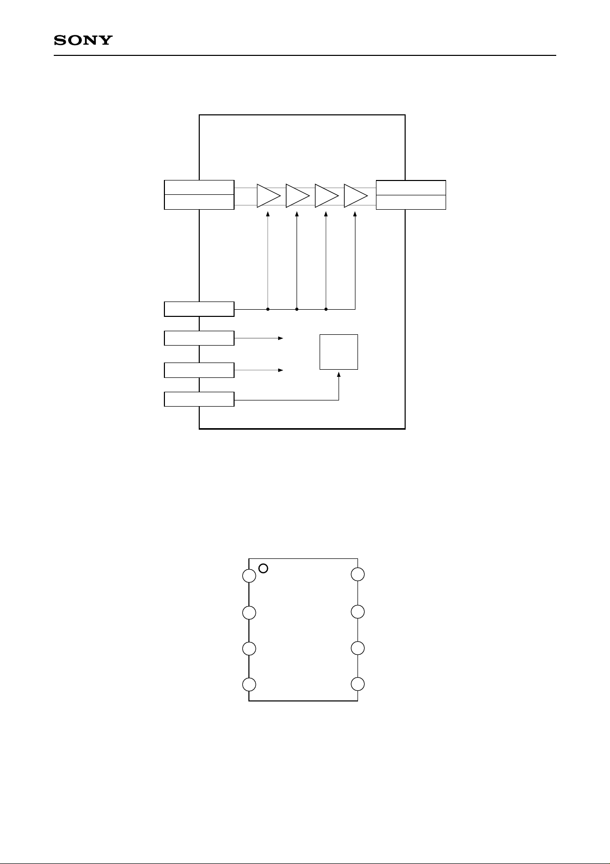
Block Diagram
CXA3222N
IF Input
Gain control
Supply Voltage
Ground
Power Save
CDMA IN
CDMA INX
GCTL
VCC
GND
PSV
Bias
Driver
OUT
OUTX
IF Output
Pin Configuration
CDMA IN
CDMA INX
GND
PSV
8
1
2
3
4
GCTL
V
CC
7
OUT
6
OUTX
5
– 2 –
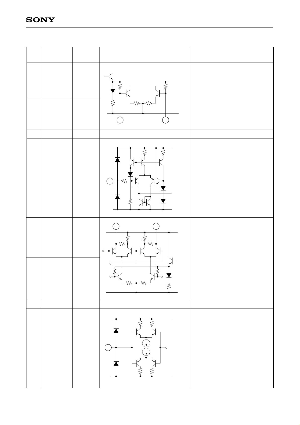
Pin Description
CXA3222N
Pin
No.
Symbol
1 CDMA IN
CDMA INX
2
3
GND
4 PSV
Pin voltage
TYP (V)
1.1
1.1
0
—
Equivalent circuit Description
40k40k
Differential input pins for CDMA
transmit IF signal.
GND
1
2
Ground.
VCC1
Power save function pin.
4
135k
High: Active
Low: Power save
5 OUTX
OUT
6
7
VCC
8 GCTL
—
—
3.0
—
5
12.25k 12.25k
8
GND
6
510510
VCC2
Differential output pins for transmit
IF signal.
Open collector output.
GND
Positive power supply.
CC1
8k8k
V
Gain control pin.
– 3 –
6k6k
GND
 Loading...