

Sony CXA3219M Datasheet
UHF-Band RF Modulator for VCR
Description
The CXA3219M is a UHF-band RF modulator which
converts the frequency of audio and video signals.
Some circuits which comprise this IC are a UHF
oscillator video clamp, white clip, video modulator,
audio FM modulator and an intercarrier SW.
Features
• Low voltage of 5V
• Wide bandwidth 470 to 750MHz
• UHF oscillator greatly reduces external parts
• Sharp white clip circuit
• Built-in voltage regulator can accept large fluctuation
of supply voltage
• Video input of 0.5Vp-p for general-purpose use
• Mixer simplifies RF unit design
• Picture/sound ratio is adjustable with external parts
• Intercarrier switch
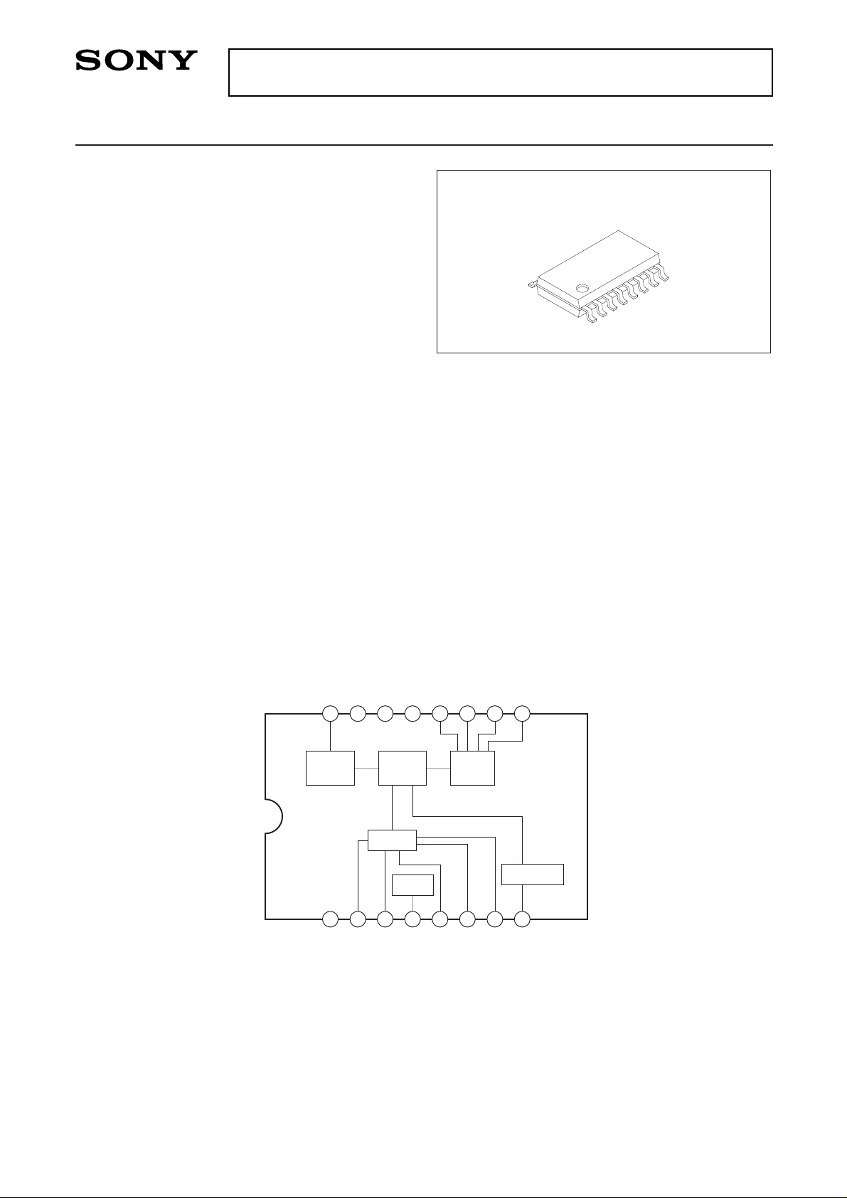
Structure
Bipolar silicon monolithic IC
Block Diagram and Pin Configuration
Applications
PAL system VCR
Absolute Maximum Ratings
• Supply voltage VCC 7V
•Operating temperature Topr –20 to +75 °C
• Storage temperature Tstg –55 to +150 °C
• Allowable power dissipation PD 350 mW
Recommended Supply Voltage Range
Supply voltage VCC 5.0 ± 0.5 V
– 1 –
E97X19-PS
Sony reserves the right to change products and specifications without prior notice. This information does not convey any license by
any implication or otherwise under any patents or other right. Application circuits shown, if any, are typical examples illustrating the
operation of the devices. Sony cannot assume responsibility for any problems arising out of the use of these circuits.
CXA3219M
16 pin SOP (Plastic)
2
3
4
5
6
7
8
9
10
11
12
13
14
15
16
1
UHF
OSC
VIDEO
MIXER
AMP
FM-OSC
REG
W/C-CLAMP
RF-OUT
ANALOG-GND
PS-ADJ
T1/T2-SW
REG
Audio-in
FM-Tank
FM-Tank
Video-in
ANALOG V
CC
OSC V
CC
OSC GND
OSC4
OSC3
OSC2
OSC1
– 2 –
CXA3219M
Pin Description and Equivalent Circuit
P/S adjustment (Adding a
capacitor between Pin 2 and
GND increases P/S ratio.)
Video modulation depth
adjustment (Adding a resistor
between Pin 2 and GND
increases the modulation
depth; adding a resistor
between Pins 2 and 4
decreases the modulation
depth.)
GND for RF/audio.
Pin
No.
1 GND1
2
P/S ADJ
1.8
Symbol
Typical pin
voltage [V]
Equivalent circuit Description
740
11.4k
2
T1/T2 SW.
T1 for GND.
T2 for OPEN.
3 T1/T2 SW 2.4
37.6k
75k
3
53.8k
Regulator output.
4 REG OUT
4.1
4
12.5k
Audio input.
5 AUDIO IN 0
5
22.5k
5.5MHz audio tank coil
connection.
6
TANK1 3.1
6
6.4k
1.6k
– 3 –
CXA3219M
6.0MHz audio tank coil
connection.
Pin
No.
7 TANK2 2.9
Symbol
Typical pin
voltage [V]
Equivalent circuit Description
7.8k
1.6k
7
Video input.
8 VIDEO IN 2.6
8
8.2k
32.4k
Oscillator pin.
9
10
11
12
OSC1
OSC2
OSC3
OSC4
2.5
1.7
1.7
2.5
8k8k
130
11
10
130
9
12
RF output.
16 RF OUT 4.1
125
1.9k
16
GND for oscillator.
Power supply for oscillator.
Power supply for RF/audio.
13
14
15
GND2
VCC1
VCC2
– 4 –
CXA3219M
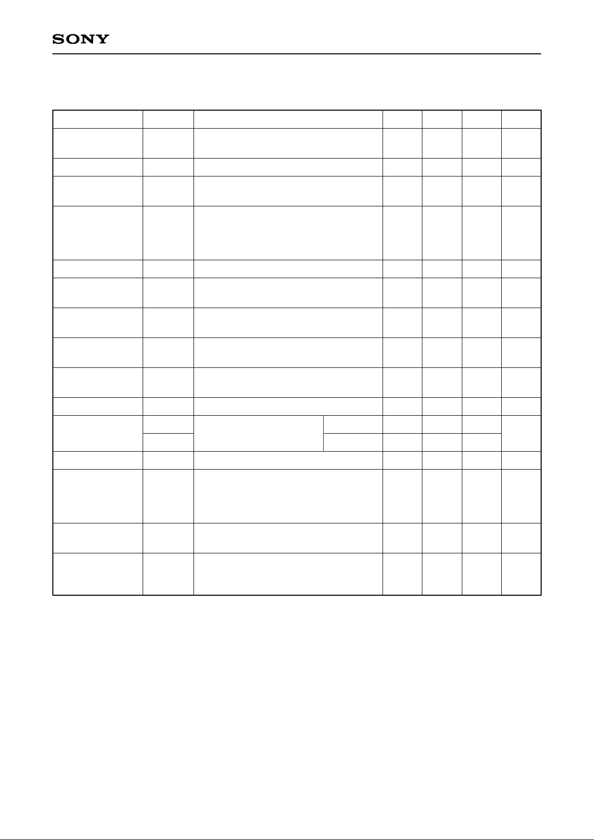
Electrical Characteristics 1
Refer to Electrical Characteristics Test Circuit. (Ta = 25°C, VCC = 5V, fP = 591.25MHz)
Item
Supply current
Video output level
Video modulation
depth
Max. video
modulation depth
(During limiter
operation)
Chroma beat
Sync crush level
Differential gain
Differential phase
Video 2nd-harmonic
wave ratio
PS ratio
Audio FM
modulation
sensitivity
Audio distortion
Audio S/N ratio
Max. audio FM
modulation depth
Audio
2nd-harmonic
wave ratio
ICC
Vo
mp
mp
(Max.)
Vcb
∆Sync
DG
DP
VVH
Vps
βS1 (T1)
βS2 (T2)
THD
ASN
ms
(Max.)
VS2
22
78.7
72
92
68
–
0
–5
48
11.5
0.400
0.380
0
45
380
52
28
81.2
78.5
95.5
78
2
1.6
0
52.5
14
0.420
0.400
0.4
54
415
57
35
83.7
86
99
–
5
5
5
–
16.5
0.455
0.440
1
–
–
–
mA
dBµV
%
%
dB
%
%
deg
dB
dB
kHz/mV
%
dB
%
dB
Symbol Conditions Min. Typ. Max. Unit
fs = 5.5MHz
fs = 6.0MHz
V1 (VIDEO IN) and V2 (AUDIO IN) at no
signal
∗1
V1 = 0.5Vp-p, FLAT FIELD signal input
V1 = 1.0Vp-p, FLAT FIELD signal input
V1 = 4.43MHz, 0.5Vp-p sine wave input
∗5
V1 = 0.5Vp-p, FLAT FIELD signal input
∆Sync = (1 – S/W • 10/4) × 100
STAIR STEP signal input
V1 = 0.5Vp-p
∗2
STAIR STEP signal input
V1 = 0.5Vp-p
∗2
V1 = 0.5Vp-p, 1MHz sine wave input
∗3
V1 = no input, fs = 5.5MHz
V2 = 100mVp-p,
1kHz sine wave input
fs frequency change/0.1V
∗6
V2 = 1kHz sine wave input
∗4
V2 = 1kHz sine wave input
0dB at fs = 5.5MHz with 60kHz deviation
V1 = STAIR STEP signal input
(rms measurement)
V2 = 1Vp-p, 1kHz sine wave input (T1)
fs frequency change (kHz)/100kHz × 100
Difference between video carrier (V1 =
no input) and 2nd-harmonic wave, at PS
ratio of 14dB conversion
– 5 –
CXA3219M
Electrical Characteristics 2
1. Video S/N
2. Video amplitude frequency characteristics
(at 1MHz reference)
3. APL variation (Normalized to APL 50%)
4. Pin 5 input impedance
5. Pin 8 input impedance
50dB (min.), 58dB (typ.)
Within ±1dB at 0.5 to 5MHz
Within ±2% at 10 to 90%
1MΩ and above
1MΩ and above
∗1
Spectrum analyzer with 50Ω input impedance should be used to test video output level. Measured value Vo
(dBm) is used to calculate output according to the following relationship:
Output (dBµ) = Vo (dBm) + 107 50Ω terminal direct reading value
∗2
Measured after demodulating by standard demodulator.
∗3
fc + 2MHz component of V1 carrier (fc) level.
∗4
Adjust the V2 level to obtain an FM deviation of ±30kHz and measure the harmonic distortion after
demodulating Vo with a standard demodulator.
∗5
Video determined by measuring ratio (dB) of chroma beat to video carrier level when V1 = no signal by
spectrum analyzer.
∗6
R1 (12kΩ) of the Electrical Characteristics Test Circuit is added for obtaining a better match between the
audio modulation sensitivity classifications and the actual pre-emphasis.
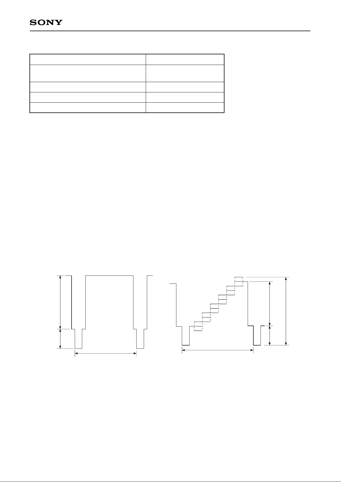
Input Waveform
90 IRE
63.5µs
40 IRE
0.5Vp-p
63.5µs
V sync
40 IRE
V white
100 IRE
FLAT FIELD signal
STAIR STEP signal
APL 50% subcarrier 20 IRE
 Loading...