

Sony CXA3218N Datasheet

—1—
E98X25-TE
Sony reserves the right to change products and specifications without prior notice. This information does not convey any license by
any implication or otherwise under any patents or other right. Application circuits shown, if any, are typical examples illustrating the
operation of the devices. Sony cannot assume responsibility for any problems arising out of the use of these circuits.
Absolute Maximum Ratings (Ta=25 °C)
• Supply voltage VCC –0.3 to 7.0 V
• Storage temperature Tstg –55 to +150 °C
• Allowable power dissipation
PD 1000 mW
Operating Conditions
• Supply voltage VCC 4.50 to 5.50 V
• Operating temperature Topr –35 to +85 °C
Description
The CXA3218N is the video signal demodulation
IC for satellite broadcasting. This IC has most of the
functions required for demodulation, and provides
stable video detection in combination with the
CXA3108Q (L-band down converter with PLL).
Features
• Built-in IF AGC
• Excellent DG/DP characteristics
• Keyed AFT input pin to support MUSE reception
• 1st AGC control output pin
• Single 5 V power supply operation
Applications
PAL/NTSC system BS tuners, etc.
Structure
Bipolar silicon monolithic IC
FM Demodulator for BS/CS
30P pin SSOP (Plastic)
CXA3218N
—2—
CXA3218N
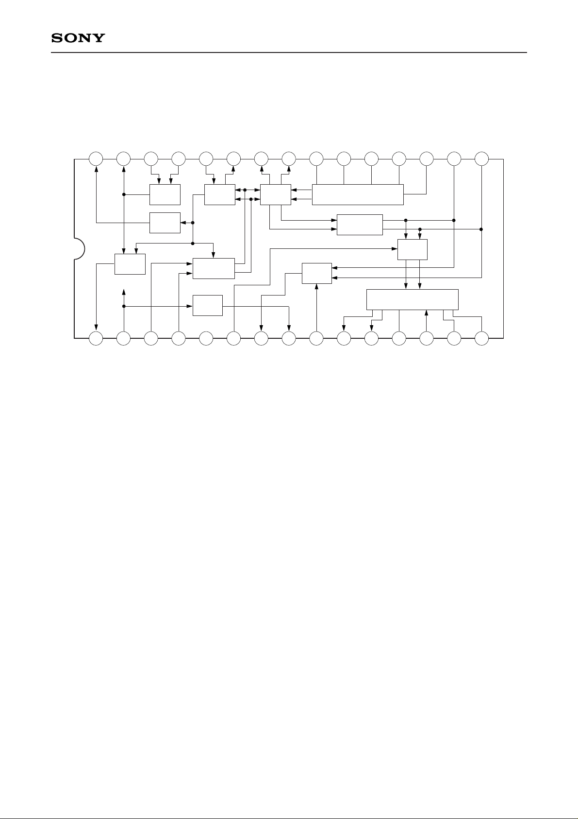
Block Diagram and Pin Configuration (Top View)
IFAGC
OPAOUT
OPAINN
OPAINP
AGCCNT
AGCLPF
LPFP
LPFN
OSCB2
OSCE2
OSCE1
OSCB1
OSCGND
VCODR1
VCODR2
MTRXAGC
V
CC
IF IN1
IF IN2
GND
OFFSET
DETOUT
VREG
GCONT
AFTDWN
AFTUP
ANA
KEYEDIN
SH2
SH1
MTRX
AGC
REG
DET
AMP
1 2 3 4 5 6 7 8 9
10 11 12 13 14 15
1AGC
2AGC
AGC
DET
161718192021222324252627282930
VCO
AFT
DCAMP
MIX
OFF
SET
AGCAMP
—3—
CXA3218N
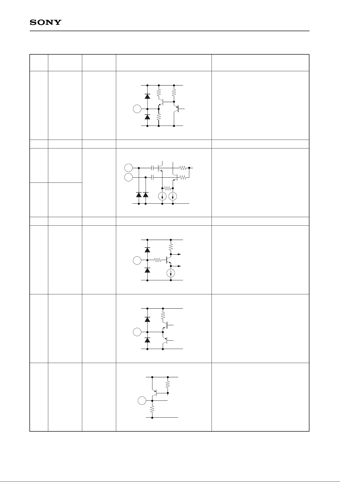
Pin Description
Pin
Symbol
Typical pin
Equivalent circuit Description
No. voltage
1
2
3
4
5
6
7
8
MTRXAGC
VCC
IF IN1
IF IN2
GND
OFFSET
DETOUT
VREG
2.0 V
to
3.5 V
5 V
0 V
2.0 V
to
4.0 V
2.45 V
4.1 V
1
100
10k
40k
VCC
GND
2.3V
GND
3
4
10p
10p
400
5k
5k
150
10k
VCC
GND
6
200
VCC
GND
7
VCC
GND
8
AGC detection block MTRX-AGC
analog output.
Positive power supply.
AGC block IF input.
Ground.
AFT block offset adjustment.
DETAMP block video output.
Reference voltage output.
Connect to GND with a 10 µF
capacitor.
—4—
CXA3218N
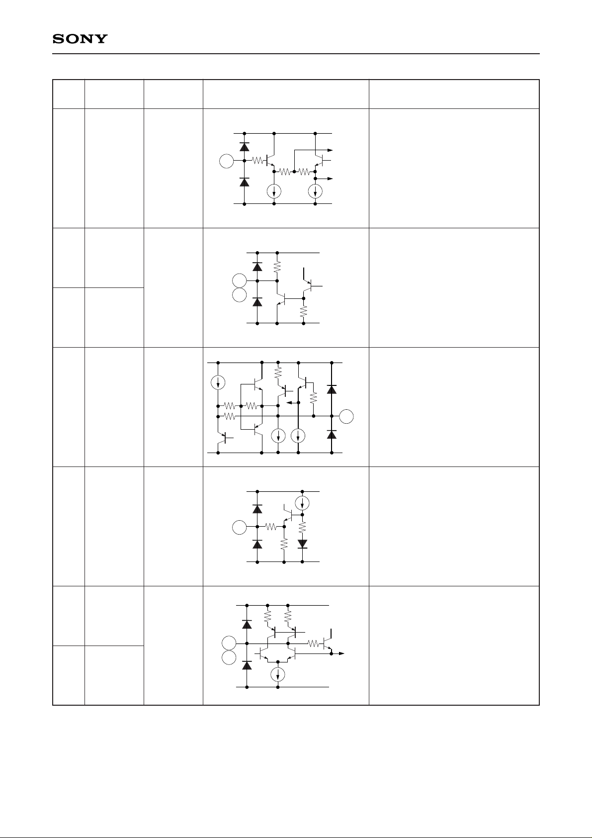
Pin
Symbol
Typical pin
Equivalent circuit Description
No. voltage
9
10
11
12
13
14
15
GCONT
AFTDWN
AFTUP
ANA
KEYEDIN
SH2
SH1
1.5 V
to
4.0 V
4.9 V
or
0.1 V
2.4 V
to
3.8 V
0.3 V
3.0 V
to
3.5 V
150
15k
VCC
GND
9
3k
2.7V
30k
30k
VCC
GND
10
11
200
47k
75k
VCC
GND
12
2k
200
2.5V
150
4k
30k
VCC
GND
13
200
2k
VCC
GND
14
15
2k
DETAMP block gain adjustment.
AFT block digital output.
AFT block filter.
Connect to GND with a 10 µF
capacitor.
AFT block keyed input.
AFT block sample-and-hold signal
output.
Connect to GND with a 0.1 µF
capacitor.
—5—
CXA3218N
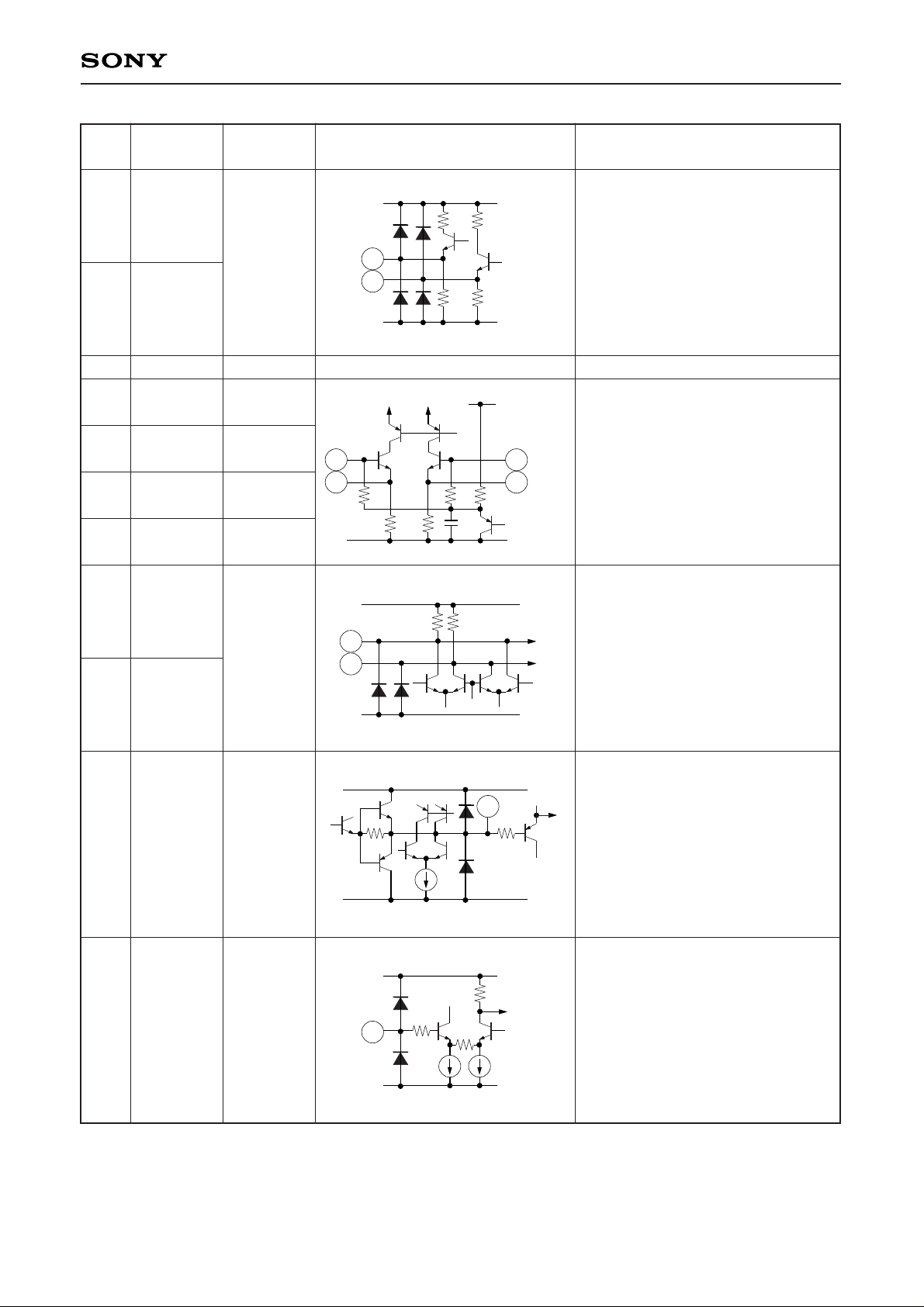
Pin
Symbol
Typical pin
Equivalent circuit Description
No. voltage
16
17
18
19
20
21
22
23
24
25
26
VCODR2
VCODR1
OSCGND
OSCB1
OSCE1
OSCE2
OSCB2
LPFN
LPFP
AGCLPF
AGCCNT
2.0 V
to
3.0 V
0 V
1.4 V
0.7 V
0.7 V
1.4 V
4.5 V
2.9 V
to
3.0 V
1.5 V
to
3.5 V
50
10k
10k
50
VCC
GND
16
17
3k 3k
VCC
OSCGND
19
2021
22
250 250
20k
260 260
VCC
GND
23
24
30k 150
V
CC
GND
25
150
45k
VCC
GND
26
PLL detection output.
Ground.
VCO resonance circuit connect
terminals.
PLL loop filter connect terminals.
AGC detection block filter.
Connect to GND with a 0.01 µF
capacitor.
AGC detection block gain adjustment.
 Loading...