

Sony CXA3205N Datasheet

—1—
E97903-TE
Sony reserves the right to change products and specifications without prior notice. This information does not convey any license by
any implication or otherwise under any patents or other right. Application circuits shown, if any, are typical examples illustrating the
operation of the devices. Sony cannot assume responsibility for any problems arising out of the use of these circuits.
Absolute Maximum Ratings (Ta = 25 °C)
• Supply voltage VCC1,VCC2 –0.3 to +5.5 V
VCC3 –0.3 to +10.0 V
• Storage temperature
Tstg –55 to +150 °C
• Allowable power dissipation
PD 880 mW
(when mounted on a substrate)
Operating Conditions
• Supply voltage VCC1, VCC2 4.75 to 5.30 V
VCC3 4.75 to 9.45 V
• Operating temperature
Topr –25 to +75 °C
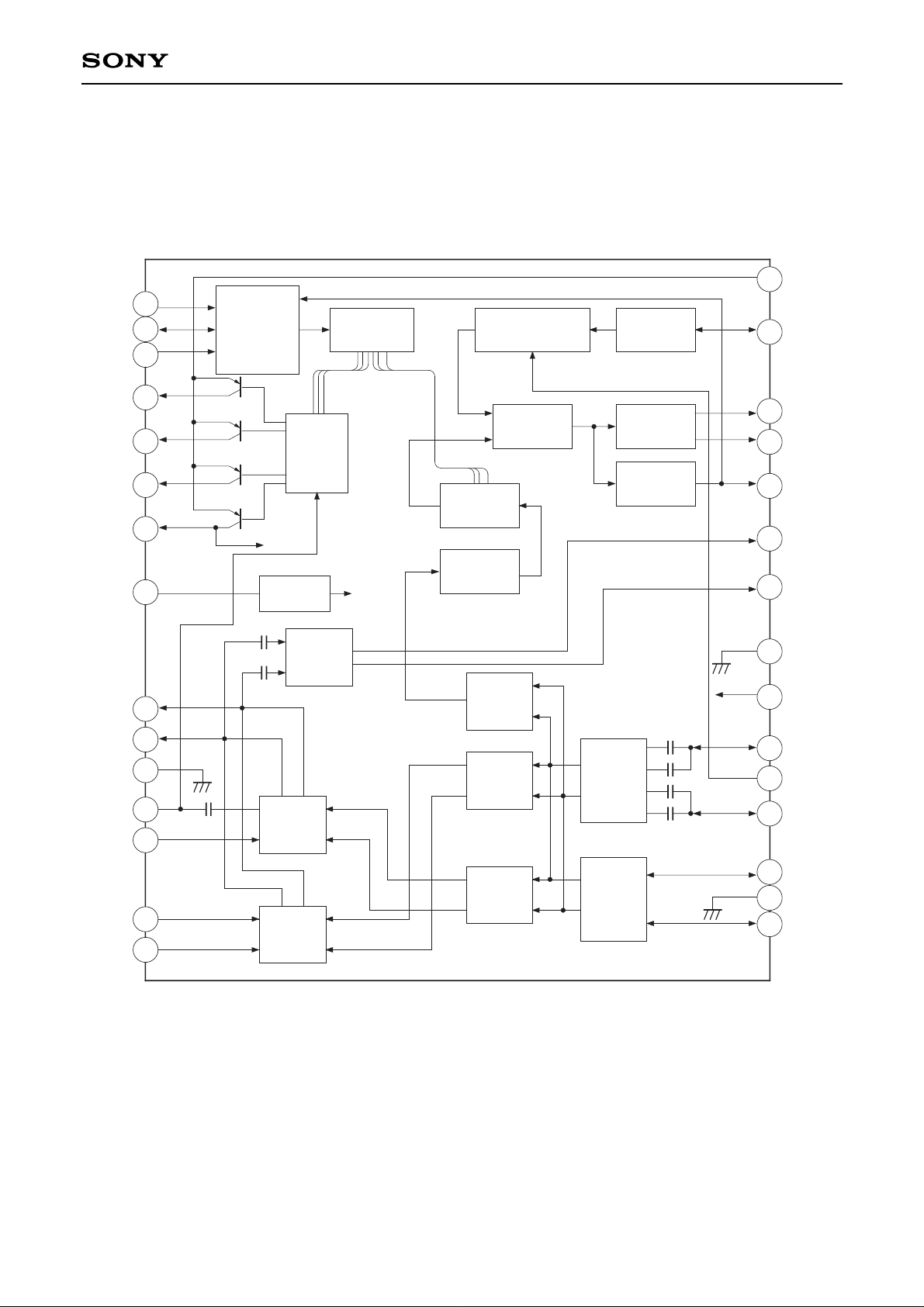
Description
The CXA3205N is a monolithic TV tuner IC which
integrates local oscillator and mixer circuits for VHF
band, local oscillator and mixer circuits for UHF
band, an IF amplifier and a tuning PLL onto a single
chip, enabling further miniaturization of the tuner.
The PLL on this IC supports the I2C bus format.
Features
• Low noise figure
• Low power consumption (5 V, 58 mA typ.)
• On-chip tuning PLL (I2C bus format)
• Selection of frequency steps 31.25 kHz, 50 kHz
and 62.5 kHz
• On-chip 4-output band switch
• IF balanced output
Applications
• TV tuners
• VCR tuners
• CATV tuners
Structure
Bipolar silicon monolithic IC
All Band TV Tuner IC with On-chip PLL
30 pin SSOP (Plastic)
CXA3205N
Note) Electrostatic discharge strength is weak, and care should be taken in handling this IC.
—2—
CXA3205N
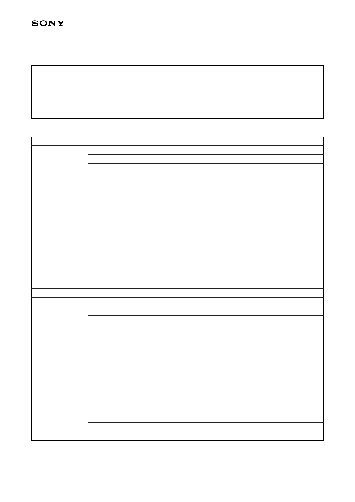
Block Diagram and Pin Configuration
Bias
USW
IF AMP
Shift
Register
Band
SW
Driver
V.REG
VHF
MIX
UHF
MIX
Buffer
VHF
OSC
UHF
OSC
Buffer
Buffer
Phase
Detector
Charge
Pump
LOCK
Det
Divider
14/15bit
Prescaler
1/8
REF
OSC
Divider
1/512,640,1024
I2C BUS
Receiver
1
2
3
4
5
6
7
8
9
10
11
12
13
14
15
16
17
18
20
21
22
23
24
25
27
28
29
19
26
30
SCL
ADSW
FMT
BVL
BVH
BU
V
CC1
MIXout1
MIXout2
GND1
BYP
VHFin
UHFin1
UHFin2
SDA
VOSC1
GND
VOSC2
UOSC1
MS
UOSC2
V
CC2
GND2
LOCK
CPO
CPE
REFOSC
V
CC3
IF OUT2
IF OUT1
—3—
CXA3205N
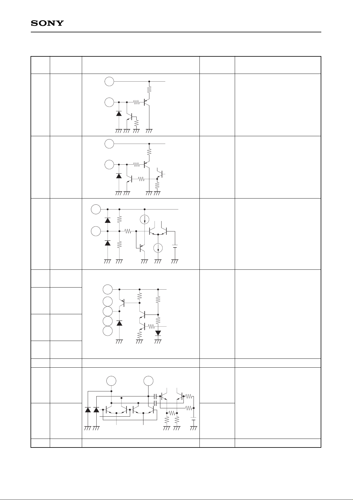
Pin Description
Pin
Symbol Equivalent circuit
Pin voltage
Description
No. (V)
1
2
3
4
5
6
7
8
9
10
11
SCL
SDA
ADSW
FMT
BVL
BVH
BU
VCC1
MIXout1
MIXout2
GND1
—
—
1.25
(when open)
ON : 4.9
OFF : 0
—
Clock input.
Data I/O.
Address selection.
This pin controls bits 2 and 1 of
the address byte.
4 : Output for FM TRAP.
5 : Power supply output for
VL band.
6 : Power supply pin for VH
band.
7 : Power supply output for
UHF band.
The pin corresponding to the
selected band goes High.
Analog circuit power supply.
Mixer outputs.
Analog circuit GND.
1
22
VCC2
100k
5k
2
22
VCC2
100k
5k
3
22
150k
50k
VCC2
4
5
6
7
30
VCC3
20k
9
10
—
—4—
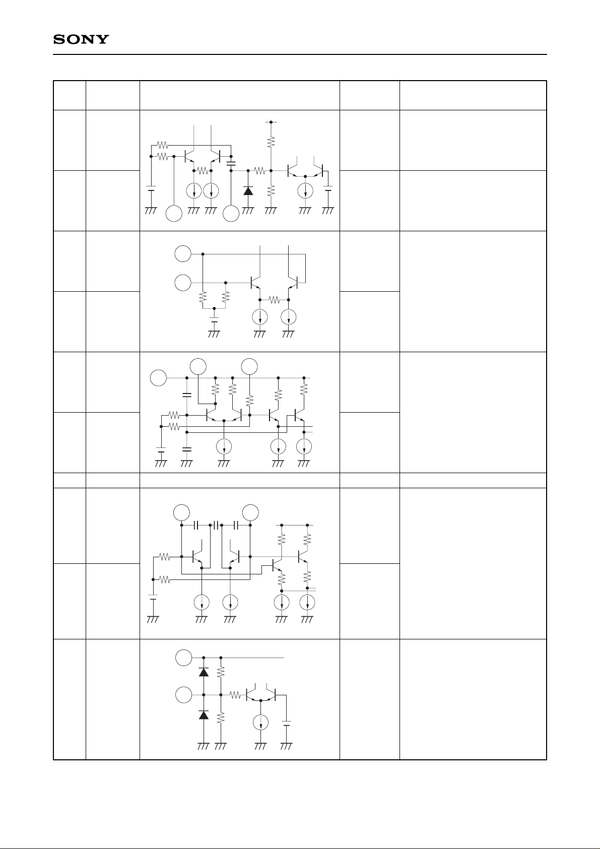
CXA3205N
Pin
Symbol Equivalent circuit
Pin voltage
Description
No. (V)
12
13
14
15
16
18
17
19
21
20
BYP
VHFin
UHFin1
UHFin2
VOSC1
VOSC2
GND
UOSC1
UOSC2
MS
3.0
(when open)
2.3
(VHF)
0
(UHF)
0
(VHF)
2.3
(UHF)
0
(VHF)
2.3
(UHF)
3
(VHF)
3.1
(UHF)
4.0
(VHF)
5.0
(UHF)
—
3.2
(VHF)
2.9
(UHF)
3.2
(VHF)
2.9
(UHF)
1.5
(when open)
VHF input GND and FMT/BU
data switching.
VHF input.
The input format is unbalanced
input.
UHF inputs.
The input method can be
selected from balanced input
or unbalanced input.
External resonance circuit
connection for VHF oscillator.
GND
External resonance circuit
connection for UHF oscillator.
Frequency step mode
selection.
Five modes can be selected
according to the applied
voltage.
20k
VCC2
80k
1213
120k
14
15
3k 3k
18 16
8
8p
3k
3k
15p
50k
50
V
CC1
19 21
3k
3k
VCC1
20
22
120k
50k
V
CC2
—5—
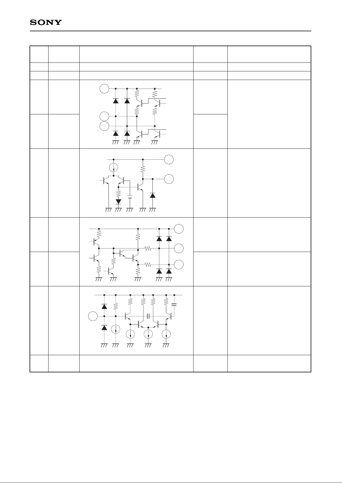
CXA3205N
Pin
Symbol Equivalent circuit
Pin voltage
Description
No. (V)
22
23
24
25
26
27
28
29
30
VCC2
GND2
IFOUT2
IFOUT1
LOCK
CPE
CPO
REFOSC
VCC3
—
—
3.0
3.0
5.0
(Lock)
0.2
(UNLock)
0.6
2.0
4.3
—
PLL circuit power supply.
PLL circuit GND.
IF outputs.
LOCK detection.
High when locked, Low when
unlocked.
NPN transistor connection for
varicap diode drive.
Charge pump output.
Connect a loop filter.
Crystal connection for
reference oscillator.
Power supply for external
supply.
VCC1
25
15
8
15
24
26
22
VCC2
40k
28
27
22
VCC2
200
500
20k
60k
29
30p
30p
—
—
—6—
CXA3205N
Electrical Characteristics See the Electrical Characteristics Measurement Circuit.
Circuit Current (VCC=5 V, Ta=25 °C)
Item
Circuit current A
Circuit current D
Symbol
AICCV
AICCU
DICC
Measurement conditions
VCC1 current, Band switch output
open during VHF operation
VCC1 current, Band switch output
open during UHF operation
VCC2 current
Min. Typ. Max. Unit
36 47 61 mA
37 48 62 mA
7 11 15 mA
Item
Conversion gain
∗1, ∗5
Noise figure ∗1,
∗2
1 % cross
modulation ∗1,
∗3
Maximum output power
Switch ON drift
∗4
Supply voltage drift
∗4
Symbol
CG1
CG2
CG3
CG4
NF1
NF2
NF3
NF4
CM1
CM2
CM3
CM4
Pomax
∆fsw1
∆fsw2
∆fsw3
∆fsw4
∆fst1
∆fst2
∆fst3
∆fst4
Measurement conditions
VHF operation fRF = 55 MHz
VHF operation fRF = 360 MHz
UHF operation fRF = 360 MHz
UHF operation fRF = 800 MHz
VHF operation fRF = 55 MHz
VHF operation fRF = 360 MHz
UHF operation fRF = 360 MHz
UHF operation fRF = 800 MHz
VHF operation
fD = 55 MHz, fUD = ±12 MHz
VHF operation
fD = 360 MHz, fUD = ±12 MHz
UHF operation
fD = 360 MHz, fUD = ±12 MHz
UHF operation
fD = 800 MHz, fUD = ±12 MHz
50 Ω load saturation output
VHF operation fOSC = 100 MHz
∆f from 3 s to 3 min after switch ON
VHF operation fOSC = 405 MHz
∆f from 3 s to 3 min after switch ON
UHF operation fOSC = 405 MHz
∆f from 3 s to 3 min after switch ON
UHF operation fOSC = 845 MHz
∆f from 3 s to 3 min after switch ON
VHF operation fOSC = 100 MHz
∆f when VCC 5 V changes ±5 %
VHF operation fOSC = 405 MHz
∆f when VCC 5 V changes ±5 %
UHF operation fOSC = 405 MHz
∆f when VCC 5 V changes ±5 %
UHF operation fOSC = 845 MHz
∆f when VCC 5 V changes ±5 %
Min. Typ. Max. Unit
24 28 31 dB
25 29 32 dB
29 33 36 dB
30 34 37 dB
12 15 dB
11 14 dB
8.5 12.5 dB
9.5 13.5 dB
97 101 dBµ
96 100 dBµ
92 96 dBµ
88 92 dBµ
+9 +14 dBm
±300 kHz
±400 kHz
±400 kHz
±500 kHz
±150 kHz
±250 kHz
±200 kHz
±250 kHz
OSC/MIX/IF Amplifier Block
—7—
CXA3205N
Item
SDA, SCL
“H” level input voltage
“L” level input voltage
“H” level input current
“L” level input current
SDA “L” output voltage
Clock input hysteresis
Clock rate
CPO (charge pump)
Output current 1
Output current 2
Leak current 1
Leak current 2
REFOSC
Oscillator frequency range
Input capacitance
Drive level
BVL, BVH, BU (Band SW)
Output current
Saturation voltage
Leak current
FMT (Band SW)
Output current
Saturation voltage
Leak current
Bus timing
SCL clock frequency
Start waiting time
Start hold time
Low hold time
High hold time
Start setup time
Data hold time
Data setup time
Rise time
Fall time
Stop setup time
Symbol
VIH
VIL
IIH
IIL
LSDA
CIHYS
CIRATE
ICPO1
ICPO2
LeakCP1
LeakCP2
FXTOSC
CXTOSC
VXTOSC
IBS1
VSAT1
LeakBS1
IBS2
VSAT2
LeakBS2
fSCL
tWSTA
tHSTA
tLOW
tHIGH
tSSTA
tHDAT
tSDAT
tR
tF
tSSTO
Measurement conditions
VIH = VCC
VIL = GND
Sink current = 3 mA
Byte4/Bit6 = 0
Byte4/Bit6 = 1
Byte4/Bit6 = 0
Byte4/Bit6 = 1
When ON
When ON Sink current = 20 mA
When OFF
When ON
When ON Sink current = 5 mA
When OFF
See Timing Chart on Page 15.
See Timing Chart on Page 15.
See Timing Chart on Page 15.
See Timing Chart on Page 15.
See Timing Chart on Page 15.
See Timing Chart on Page 15.
See Timing Chart on Page 15.
See Timing Chart on Page 15.
See Timing Chart on Page 15.
See Timing Chart on Page 15.
Min. Typ. Max. Unit
3 VCC V
GND 1.5 V
0 –0.1 µA
–1 –2 µA
0.4 V
0.25 0.4 0.65 V
0.5 MHz
±35 ±50 ±75 µA
±140 ±200 ±300 µA
30 nA
100 µA
3 12 MHz
17.5 19 20.5 pF
200 400 mVp-p
–25 mA
100 200 mV
0.5 3 µA
–7 mA
75 150 mV
0.03 0.1 µA
0 400 kHz
1300 ns
600 ns
1300 ns
600 ns
600 ns
1300 ns
600 ns
300 ns
300 ns
600 ns
PLL Block
∗1
Measured value for untuned inputs.
∗2
Noise figure is the direct-reading value of NF meter in DSB.
∗3
Desired signal (fD) input level is –30 dBm. Undesired signal (fUD) is 100 kHz, 30 % AM at ±12 MHz.
The measurement value is undesired signal level, it measured with a spectrum analyzer at S/I=46 dB.
∗4
Value when the PLL is not operating.
∗5
Loss caused by external parts connected to Pins 24 and 25 is compensated.
This is the value converted to IC output pin amplitude.
 Loading...