

Sony CXA3199TN Datasheet
—1—
E98221-TE
Sony reserves the right to change products and specifications without prior notice. This information does not convey any license by
any implication or otherwise under any patents or other right. Application circuits shown, if any, are typical examples illustrating the
operation of the devices. Sony cannot assume responsibility for any problems arising out of the use of these circuits.
Absolute Maximum Ratings (Ta=25 °C)
• Supply voltage VCC 6V
•Operating temperature Topr –20 to +70 °C
• Storage temperature Tstg –55 to +150 °C
• Allowable power dissipation (on board)
PD 1000 mW
Operating Conditions
Supply voltage VCC 3.1 to 5.5 V
Description
The CXA3199TN is a wideband Pre-amplifier for
VTR head.
Features
• Operate on single +3.3 V power supply
• Low power consumption
Read : 45 mW
• Ultra small package
• Wideband (–3 dB) : 140 MHz (typ)
• Read amplifier emitter follower output featuring
380 times gain (typ).
• Low input capacitance : 3.0 pF
• Low input noise : 0.65 nV /√ Hz
• Read data outputs are high impedance in Power
Saving Mode
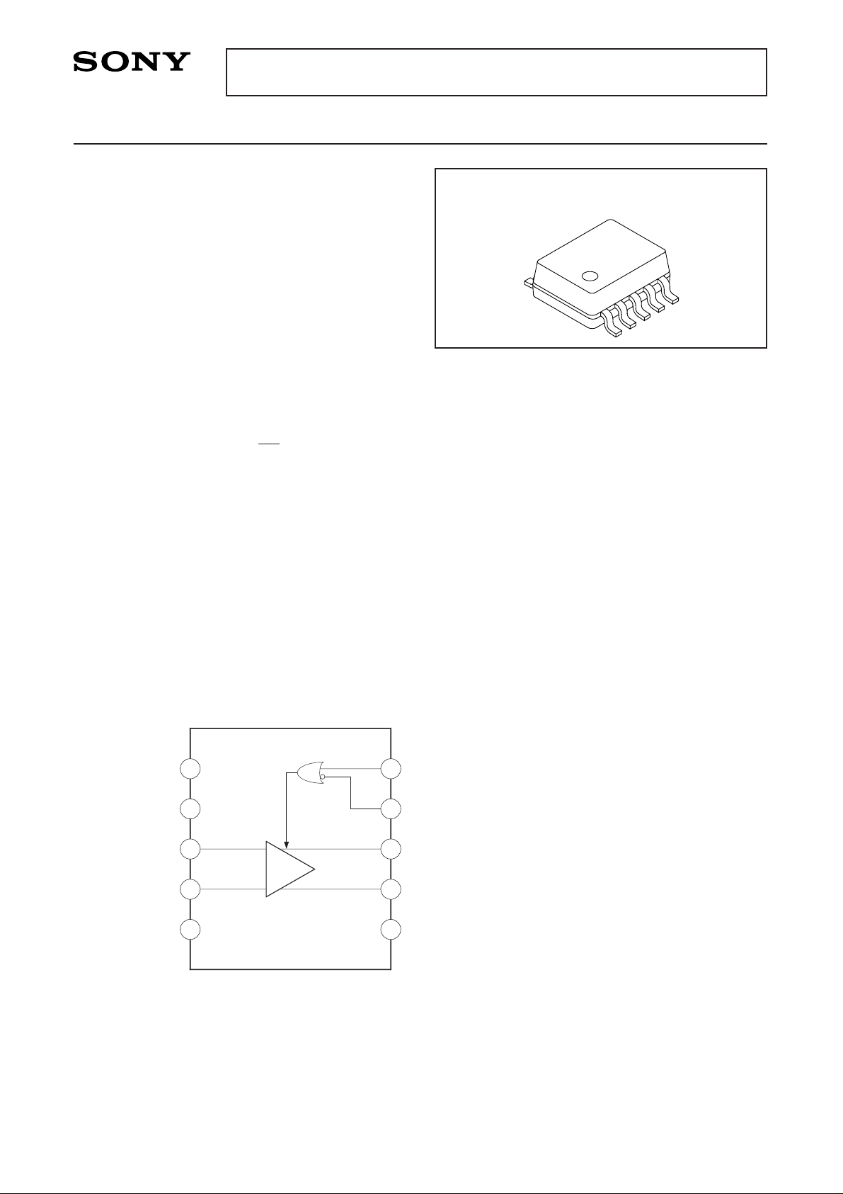
Structure
Bipolar silicon monolithic IC
Wideband Pre-amplifier
10 pin TSSOP (Plastic)
CXA3199TN
Block Diagram and Pin Configuration
NC
HX
HY
GND
V
CC
RDY
RDX
CE
XCE
GND
AMP
1
2
3
4
5
10
9
8
7
6
—2—
CXA3199TN
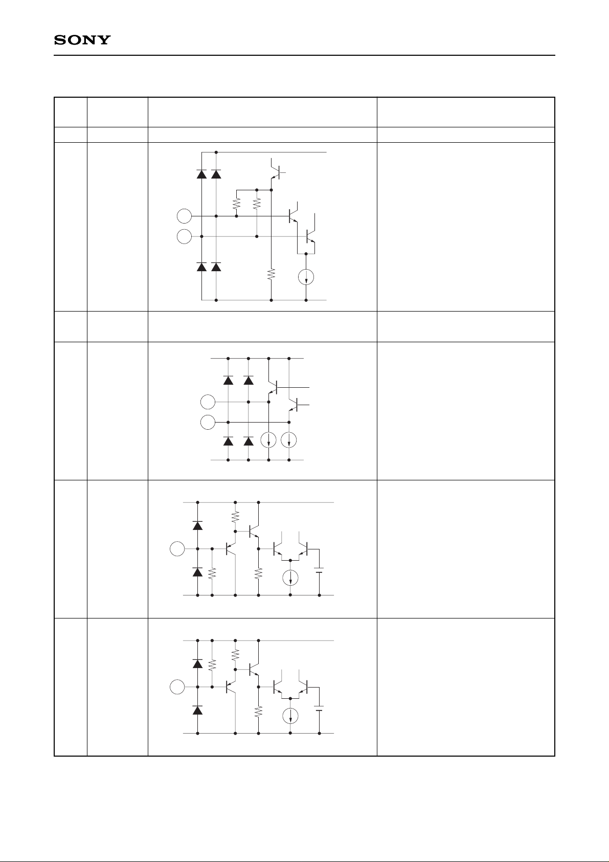
Pin Description
No. Symbol Equivalent circuit Description
1
3
4
5
6
7
8
9
10
VCC
H0X
H0Y
GND
RDY
RDX
XCE
CE
Head.
Read amplifier output.
Power Save signal input.
Power Save signal input.
2k 2k
VCC
GND
100k
4
3
VCC
GND
7
8
VCC
GND
9
100k
50k
1.6V
100k
VCC
GND
100k
50k
1.6V
100k
10

—3—
CXA3199TN
Electrical Characteristics (Unless otherwise specified, VCC=3.3 V, Ta=25 °C)
Item
Current consumption for read
Current consumption for chip
disenable
Digital input
“Low” input voltage
Digital input
“High” input voltage
Digital input
“Low” input current
Digital input
“High” input current
Read amplifier differential
voltage gain
Frequency band width
(–3 dB)
Input referred noise voltage
Common mode rejection ratio
Supply voltage rejection ratio
Read data output offset voltage
for Read
Chip disenable to read
Differential input capacitance
Differential input resistance
Output resistance
Read data output sink current
Symbol
ICCR
ICCXCE
VIL
VIH
IIL
IIH
AV
BW
EN
CMRR
PSRR
VOFFR
TIR
CIN
RIN
RRD
Isink
Test condition
“H” applied voltage: 3.3 V
“L” applied voltage: 0 V
Input voltage :
1 mVp-p, 300 kHz
Frequency at which AV lower
by 3 dB
Head impedance : 0 Ω
Common input voltage :
100 mVp-p, 20 MHz
Ripple voltage :
100 mVp-p, 20 MHz
VOFFR=VRDX–VRDY, A version
RDX or RDY
Min. Typ. Max. Unit.
8.0 13.5∗19.5 mA
0.3 0.5 0.8 mA
0.8 V
2.0 V
–100 µA
100 µA
300 380 460 V/V
100 145 MHz
0.65 0.8
nV
√ Hz
50 dB
50 dB
–300 300 mV
500 ns
3.0 4.5 pF
0.8 2.1 3.5 kΩ
10.0 20.0 35.0 Ω
2.0 3.0 4.1 mA
∗ Guaranteed until Ta=70°C
—4—
CXA3199TN
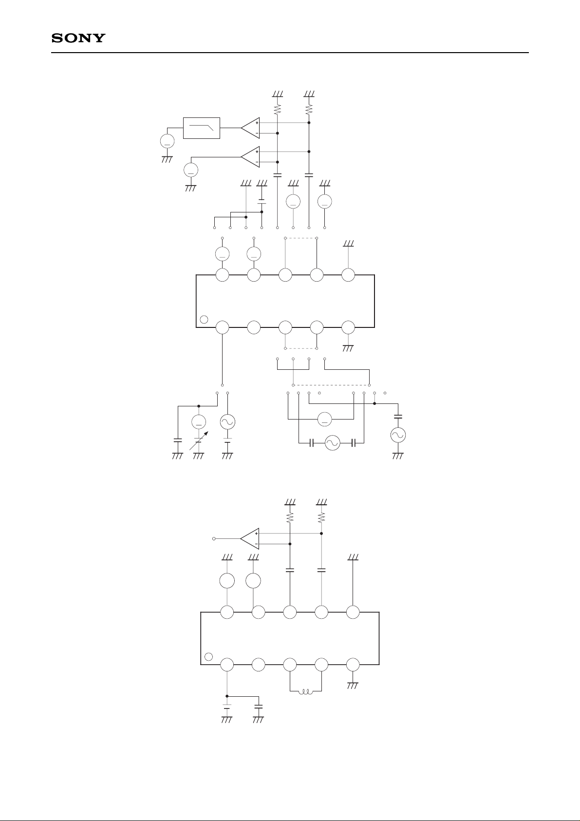
Test Circuit 1
×100
×1
baa b a b
A A
1µ
1k
1µ
1k
AMP
V
AMP
V
LPF
V V
ba
a b a b
ab cba d
0.1µ
1 2 3 4 5
cba d
A
0.1µ
0.1µ
A
1µ
a
910 678
to 50MHz
3.3V
V
CC
3.3V
VCC
3.3V
Test Circuit 2
×1
PG
1µ
1k
1µ
1k
AMP
LH
1µH
PG
1 2 3 4 5
9
10
8 7 6
1µ3.3V
 Loading...