

Sony CXA3197R Datasheet
10-bit 125MSPS D/A Converter
Description
The CXA3197R is a high-speed D/A converter
which can perform multiplexed input of two system
10-bit data.
This IC realizes a maximum conversion rate of
125MSPS. Multiplexed operation is possible by
inputing the 1/2 frequency-divided clock or by halving
the frequency of the clock internally with the clock
frequency divider circuit having the reset pin. The
data input is at TTL level, and the clock input and
reset input can select either TTL or PECL level
according to the application.
Features
• Maximum conversion rate:
During PECL operation: 125MSPS
During TTL operation: 100MSPS
• Resolution: 10 bits
• Low power consumption: 480mW (typ.)
• Data input level: TTL
• Clock, reset input level: TTL and PECL compatible
• 2:1 multiplexed input function
• 1/2 frequency-divided clock output possible by the
built-in clock frequency divider circuit
• Voltage output (50Ω load drive possible)
• Single power supply or ±dual power supply operation
• Reset signal polarity switching function
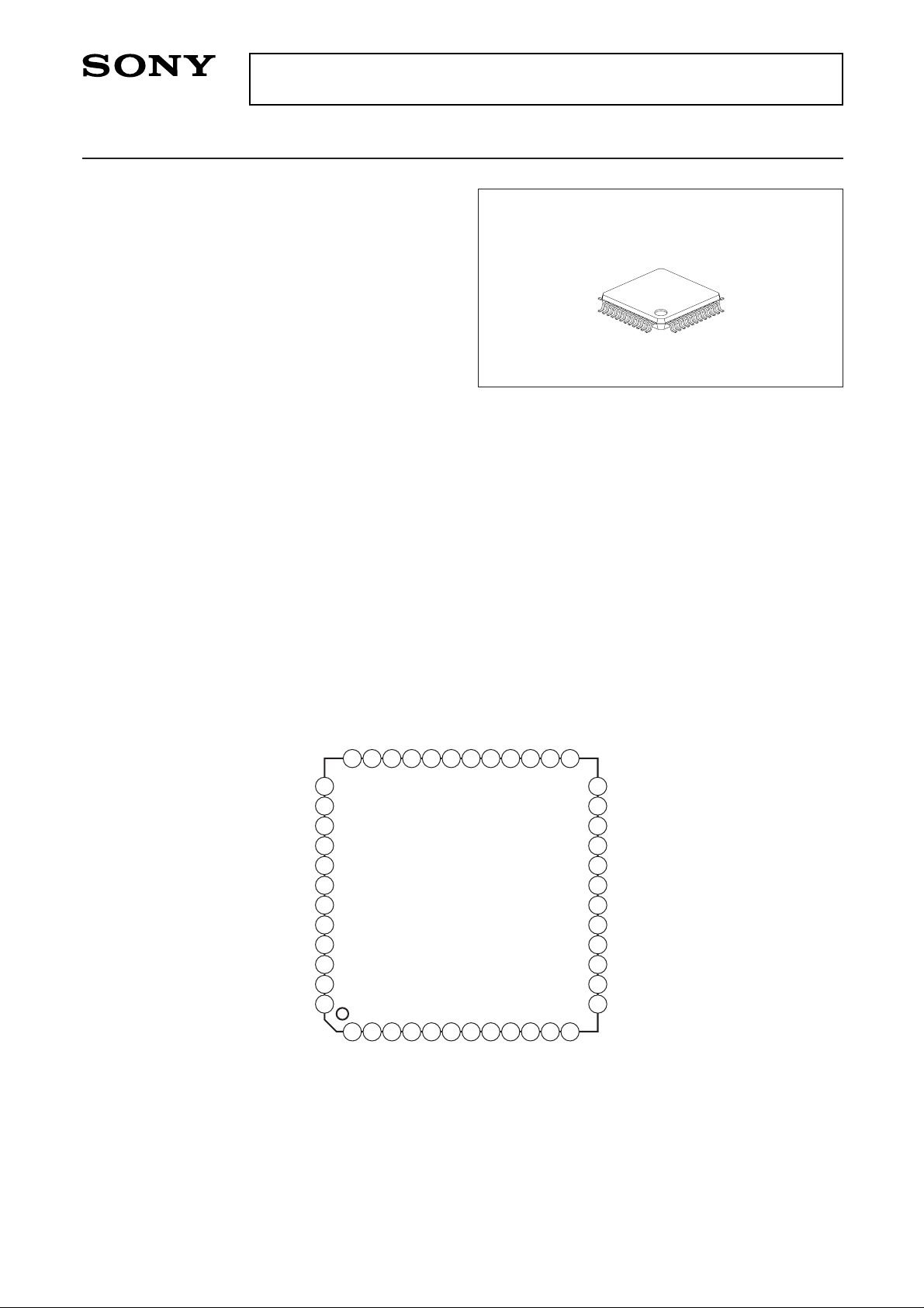
Pin Configuration
Structure
Bipolar silicon monolithic IC
Applications
• LCD
• DDS
• HDTV
• Communications (QPSK, QAM)
• Measuring devices
– 1 –
E97639-PS
Sony reserves the right to change products and specifications without prior notice. This information does not convey any license by
any implication or otherwise under any patents or other right. Application circuits shown, if any, are typical examples illustrating the
operation of the devices. Sony cannot assume responsibility for any problems arising out of the use of these circuits.
CXA3197R
48 pin LQFP (Plastic)
13
14
15
16
17
18
19
20
21
22
23
24
25
26
2728
29
30
36
35
34
31
32
33
40
39
38
37
41
42
43
44
45
46
47
48
2
3
4
5
6
7
8
9
10
11
12
1
DA5
DA4
DA3
DA2
DA1
(LSB) DA0
(MSB) DB9
DB8
DB7
DB6
DB5
DB4
AV
CC
2
VSET
VREF
AGND2
AOUTP
AV
CC
O
AOUTN
DV
CC
2
C3
C2
C1
DGND2
DB3
DB2
DB1
DB0 (LSB)
DIV2IN
DIV2OUT
CLK/T
CLKP/E
CLKN/E
RESET/T
RESETP/E
RESETN/E
DA6
DA7
DA8
(MSB) DA9
DGND1
N.C.
DV
CC1
PS
INV
R POLARITY
VOCLP
AGND2
LEAD TREATMENT: PALLADIUM PLATING
– 2 –
CXA3197R
Absolute Maximum Ratings (Ta = 25°C)
• Supply voltage AVCCO, AVCC2, DVCC2 –0.5 to +6.0 V
AGND2, DGND2 –6.0 to +0.5 V
DVCC1 –0.5 to +6.0 V
AVCC2 – AGND2 –0.5 to +6.0 V
AVCCO – AGND2 –0.5 to +6.0 V
DVCC2 – DGND2 –0.5 to +6.0 V
• Input voltage
(Analog) VSET AGND2 – 0.5 to AVCC2 + 0.5 V
(Digital) TTL input pin DGND1 – 0.5 to DVCC1 + 0.5 V
PECL input pin DGND1 – 0.5 to DVCC1 + 0.5 V
PS DGND1 – 0.5 to DVCC1 + 0.5 V
(Others) VOCLP DGND1 – 0.5 to DVCC1 + 0.5 V
• Storage temperature Tstg – 65 to +150 °C
• Allowable power dissipation Pd 1.4 W
(when mounted on a two-layer glass fabric base epoxy board with dimensions of 76mm × 114mm, t = 1.6mm)
Recommended Operating Conditions
[Single power supply] [Dual power supply]
• Supply voltage Min. Typ. Max. Min. Typ. Max. Unit
AVCCO +4.75 +5.0 +5.25 –0.05 0.0 +0.05 V
AVCC2 +4.75 +5.0 +5.25 –0.05 0.0 +0.05 V
AGND2 –0.05 0.0 +0.05 –5.50 –5.0 –4.75 V
DVCC1 +4.75 +5.0 +5.25 +4.75 +5.0 +5.25 V
DGND1 –0.05 0.0 +0.05 –0.05 0.0 +0.05 V
DVCC2 +4.75 +5.0 +5.25 –0.05 0.0 +0.05 V
DGND2 –0.05 0.0 +0.05 –5.50 –5.0 –4.75 V
• Input voltage Min. Typ. Max. Unit
(Analog) VSET AGND2 + 0.65 AGND2 + 1.03 V
(Digital) TTL input pin VIH DGND1 + 2.0 V
VIL DGND1 + 0.8 V
PECL input pin VIH DVCC1 – 1.05 DVCC1 – 0.5 V
VIL DVCC1 – 3.2 DVCC1 – 1.4 V
VID
∗1
0.5 0.8 V
(Others) VOCLP DGND1 + 2.4 DVCC1 V
• CLK pulse width (for RECL CLK) tpw1 3.5 ns
tpw0 3.5 ns
• Maximum conversion rate During PECL operation Fc 125 MSPS
During TTL operation Fc 100 MSPS
• Load resistance RL 50 50 ≥ 10k Ω
• Analog output full-scale voltage
RL ≥ 10kΩ VFS 1.5 2.0 2.1 V
RL = 50Ω VFS 0.75 1.0 1.05 V
• Operating temperature Ta –20 +75 °C
∗1
VID: Input Voltage Differential
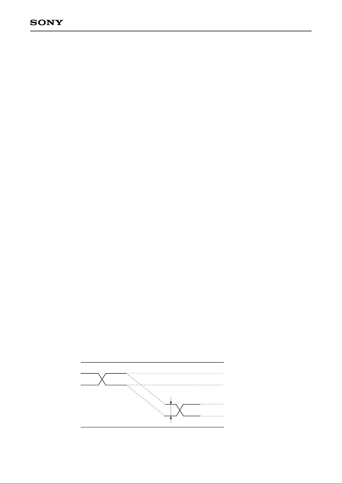
PECL input signal switching level
VIH
VIL (Min.)
V
IH (Max.)
V
IL
DVCC1
VID
DGND1

– 3 –
CXA3197R
Pin Description
[Symbol] [Pin No.] [Description]
DA0 to DA9 1 to 6, 45 to 48 Side A data input. TTL TTL
DB0 to DB9 7 to 16 Side B data input. TTL TTL
DIV2IN 17 1/2 frequency-divided clock input. TTL TTL
DIV2OUT 18 1/2 frequency-divided clock output. TTL TTL
CLK/T 19 TTL clock input. TTL TTL
CLKP/E 20 PECL clock input. PECL PECL
CLKN/E 21 PECL clock input. PECL PECL
RESET/T 22 TTL reset input. TTL TTL
RESETP/E 23 PECL reset input. PECL PECL
RESETN/E 24 PECL reset input. PECL PECL
DGND2 25 Digital ground. 0V –5V
C1 26 Function setting. TTL TTL
C2 27 Function setting. TTL TTL
C3 28 Function setting. TTL TTL
DVCC2 29 Digital power supply. 5V 0V
AVCCO 30 Analog output power supply. 5V (typ.) 0V (typ.)
AOUTN 31 Negative analog output. AVCCO – VFS AVCCO – VFS
AOUTP 32 Positive analog output. AVCCO – VFS AVCCO – VFS
AGND2 33 Analog ground. 0V –5V
VREF 34 Analog reference voltage. AGND2 + 1.25V AGND2 + 1.25V
VSET 35 Full-scale adjustment.
AVCC2 36 Analog power supply. 5V 0V
AGND2 37 Analog ground. 0V –5V
VOCLP 38 TTL High level clamp. Clamp voltage Clamp voltage
R POLARITY 39 Reset signal polarity switching. TTL TTL
INV 40 Analog output inversion. TTL TTL
PS 41 Power saving. TTL TTL
DVCC1 42 Digital power supply. 5V 5V
N.C. 43 Not connected. — —
DGND1 44 Digital ground. 0V 0V
[
Typical voltage level for
]
a single power supply
[
Typical voltage level
]
for dual power supply
AGND2 + 0.65V
to
AGND2 + 1.03V
AGND2 + 0.65V
to
AGND2 + 1.03V
– 4 –
CXA3197R
Block Diagram
VSET
VREF
29
DVCC2
28
C3
27
C2
26
C1
25
DGND2
DIV2IN
CLK/T
CLKP/E
CLKN/E
RESET/T
RESETP/E
RESETN/E
44
DGND1
42
DV
CC1
41
PS
40
INV
R POLARITY
38
VOCLP
AOUTP
AV
CCO
AOUTN
36
AVCC2
Input Latch
B
10bit 10bit
Input Latch
A
10bit 10bit
MUX
10bit
Latch
10bit
BGR
35
34
Current
Cont.
1 to 6
45 to 48
7 to 16
DA0 to DA9
DB0 to DB9
AGND2
RO = 50Ω
30
31
32
D Q
Q
22
23
24
39
AGND2
33
37
17
19
20
21
18
DIV2OUT

– 5 –
CXA3197R
Pin Description and I/O Pin Equivalent Circuit
Side A data input.
Side B data input.
1/2 frequency-divided
clock input.
Use this pin in MUX.1A
or MUX.2 mode.
Leave open for other
modes.
1/2 frequency-divided
clock output.
The 1/2 frequencydivided clock signal
(DIV2OUT) is output in
MUX.1A mode.
Set to high impedance
for other modes.
DA0 to DA9
DB0 to DB9
DIV2IN
DIV2OUT
TTL
TTL
TTL
TTL
1 to 6
45 to 48
7 to 16
17
18
I
I
I
O
DVCC1
DGND1
6
1
45
48
7
16
to
to
to
1.5V
DVCC1
DGND1
17
1.5V
DVCC1
DGND1
18
100K
Clock input.
Use this pin when the
clock is input at TTL
level.
At this time, leave Pins
20 and 21 open.
CLK/T TTL19 I
DVCC1
DGND1
19
1.5V
Pin No. Symbol
Typical voltage level
Equivalent circuit DescriptionI/O

– 6 –
CXA3197R
Clock input.
Use this pin when the
clock is input at PECL
level.
At this time, leave
Pin 19 open.
CLKP/E and CLKN/E
are complementary and
should be used together.
CLKP/E complementary
input.
Reset signal input.
When multiple
CXA3197R are
operated at the same
time in MUX.1A or
MUX.1B mode, the start
timing of the internal 1/2
frequency divider
circuits should be
matched.
At this time, the reset
signal is used; when the
reset signal is at TTL
level, Pin 22 is used and
Pins 23 and 24 are left
open. When the reset
signal is at PECL level,
Pins 23 and 24 are used
and Pin 22 is left open.
The reset signal polarity
can be set by Pin 39
(R POLARITY).
Leave the reset pin
open when other modes
are used.
RESETP/E and
RESETN/E are
complementary and
should be used together.
CLKP/E PECL20
I
CLKN/E PECL
21
I
RESET/T
TTL
22
I
RESETP/E PECL23 I
RESETN/E
PECL
24
I
DGND2
Single power
supply: GND
Dual power
supply: –5V
25
DVCC1
DGND1
20
21
Function setting.
Function setting.
Function setting.
C1 TTL26 I
C2 TTL27 I
C3
TTL
28
I
26
28
DVCC1
DGND1
27
1.5V
DVCC1
DGND1
22
1.5V
DVCC1
DGND1
23
24
Digital power supply.
Pin No. Symbol
Typical voltage level
Equivalent circuit DescriptionI/O
– 7 –
CXA3197R
DVCC2
29
32
AVCCO
AGND2
31
RORO
Digital power supply.
Analog output power
supply.
The AVCCO pin voltage
can be varied within the
range that satisfies the
analog output
compliance voltage.
Positive analog output.
Analog ground.
Negative analog output.
The inverse of the
positive analog output
pin is output.
When the positive
output is terminated with
50Ω, the inverse output
pin should also be
terminated with 50Ω
even if the inverse
output is not used.
AVCCO
Single power
supply: +5V
Dual power
supply: GND
30
AOUTN
AVCCO – VFS
31
O
AOUTP
AVCCO – VFS
32
O
Single power
supply: +5V
Dual power
supply: GND
Reference voltage
output.
AVCC2
AGND2
34
BGR
AGND2
Single power
supply: GND
Dual power
supply: –5V
33
VREF
AGND + 1.25V
(Typ.)
34
O
Analog output full-scale
adjustment.
VSET
AGND2 + 0.65V
to
AGND2 + 1.03V
35 I
AVCC2
35
AGND2
Pin No. Symbol
Typical voltage level
Equivalent circuit DescriptionI/O
AVCC2
36
Analog power supply.
Single power
supply: +5V
Dual power
supply: GND

– 8 –
CXA3197R
TTL output High level
clamp.
A TTL level signal is
output from the
DIV2OUT pin in
MUX.1A mode. The
TTL High level voltage
can be clamped to the
value approximately
equivalent to the voltage
applied to this pin.
Leave the VOCLP pin
open for other modes.
VOCLP
Clamp voltage
38
I
DVCC1
DGND1
38
Reset signal polarity
switching.
At High level, the reset
polarity is active Low; at
Low level, active High.
R POLARITY
TTL
39
I
DVCC1
DGND1
39
1.5V
Analog output polarity
inversion.
The analog output is
inverted at Low level.
INV TTL
40
I
DVCC1
DGND1
40
1.5V
Power saving.
Power saving mode is
activated at Low level.
Normally pull up the PS
pin to High level as this
pin is open Low.
PS TTL41 I
DVCC1
42
DVCC1
DGND1
41
Digital power supply.
5V
N.C.
43
Not connected.
DGND1
44
Digital ground.
0V
Pin No. Symbol
Typical voltage level
Equivalent circuit DescriptionI/O
Analog power supply.
AGND2
Single power
supply: GND
Dual power
supply: –5V
37
– 9 –
CXA3197R
Resolution
Differential linearity error
Integral linearity error
Digital input (PECL)
Digital input voltage
Digital input current
Digital input capacitance
Digital input (TTL)
Digital input voltage
Threshold voltage
Digital input current
Digital input capacitance
Digital output (TTL)
Digital output voltage
Leak current at high impedance
Digital output rise time
Digital output fall time
PS pin input (PS)
PS pin input voltage
PS pin input current
Clamp pin (VOCLP)
VOCLP pin input current
Analog output characteristics
Output full-scale voltage
: RL ≥ 10kΩ
: RL = 50Ω
Output zero offset voltage
: RL ≥ 10kΩ
: RL = 50Ω
Analog output resistance
Analog output capacitance
Absolute amplitude error
Absolute amplitude error
temperature characteristics
Analog output rise time
Analog output fall time
Settling time
Glitch energy
Compliance voltage
n
DLE
ILE
VIH
VIL
IIH
IIL
VIH
VIL
VTH
IIH
IIL
VOH
VOL
Tr
Tf
VIH
VIL
IIH
IIL
IVOCLP
IVOCLP
VFS
VFS
VOF
VOF
RO
CO
EG
TCG
Tr
Tf
tSET
GE
VOC
VFS = 1000mV
∗2
VIH = DVCC1 – 0.8V
VIL = DVCC1 – 1.6V
VIH = 3.5V
VIL = 0.2V
IOH = –2.0mA
IOL = 1.0mA
When VO = 5V
When VO = 0V
0.8 to 2.4V (CL = 10pF)
0.8 to 2.4V (CL = 10pF)
VIH = 3.5V
VIL = 0.2V
VOCLP = DVCC1
VOCLP = 2.4V
VSET = AGND2 + 937.5mV
VSET = AGND2 + 937.5mV
VFS = 1000mV at 25°C
When RL = 50Ω,
VFS = 1V,10 – 90%
Mesured to DVCC2
∗3
10
DVCC1 – 1.05
DVCC1 – 3.2
0
–30
2
–1
–2
2.4
10
–1
1
0.6
2
1
–1
0
–60
1.5
0.75
0
0
–4.0
0.85
0.75
–2.1
10
1.5
2
1
50
10
10
–0.85/+0.5
–1.2/+0.5
±1.2
DVCC1 – 0.5
DVCC1 – 1.4
20
0
5
0.8
1
0
5
0.5
100
1
1.5
1.2
0.8
100
0
5
–10
2.1
1.05
20
10
4.0
60
1.05
0.85
3.5
5
1.5
bit
LSB
LSB
LSB
V
V
µA
µA
pF
V
V
V
µA
µA
pF
V
V
µA
µA
ns
ns
V
V
µA
µA
µA
µA
V
V
mV
mV
Ω
pF
% of F.S.
ppm/°C
ns
ns
ns
pVsec
V
Electrical Characteristics
(DVCC1, DVCC2, AVCC2, AVCCO = +5V, DGND1, DGND2 = 0V, Ta = 25°C)
Item
Symbol
Conditions
Min.
Typ.
Max. Unit
}
}
 Loading...