Sony CXA3174N Datasheet

—1—
E96932A8Z
Sony reserves the right to change products and specifications without prior notice. This information does not convey any license by
any implication or otherwise under any patents or other right. Application circuits shown, if any, are typical examples illustrating the
operation of the devices. Sony cannot assume responsibility for any problems arising out of the use of these circuits.
Absolute Maximum Ratings (Ta = 25 °C)
• Supply voltage VCC 14 V
• Operating temperature range
Topr –35 to +80 °C
• Storage temperature range
Tstg –65 to +150 °C
Operating Conditions
Supply voltage VCC 2.7 to 3.3 V
Description
The CXA3174N is a 4-bit digital control variable
gain amplifier suitable for the communications.
Features
• Gain control amplifier with the wide gain variable
range
• Doubler circuit for the LO (local) signal eliminates
need for the phase shifter
Functions
• IF signal gain control circuit
• I/Q quadrature demodulator
• Doubler circuit for the LO signal
• Gain control by the 4-bit digital data
• Power saving
Applications
GSM and PCS portable telephones
Structure
Bipolar silicon monolithic IC
AGC IF for GSM/PCS
20 pin SSOP (Plastic)
CXA3174N
Block Diagram and Package Outline
Reg
QXOUT
QOUT
LOIN
NC
VC4
VC3
VC2
VC1
NC
NC
IXOUT
IOUT
NC
NC
GND
V
CC
IFIN
IFINX
NC
PS
× 2
Gain Control AMP
1 3 4 5 6 7 8 9 102
11121314151617181920
Gain Cont
Phase
Shifter
For the availability of this product, please contact the sales office.

—2—
CXA3174N
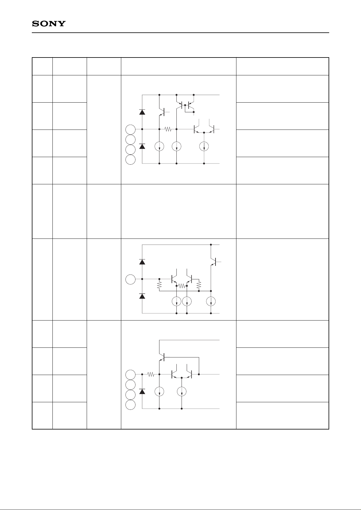
Pin Description
Pin
Symbol Pin voltage Equivalent circuit Description
No.
1
2
19
20
3
5
10
12
17
18
4
6
7
8
9
QXOUT
QOUT
IOUT
IXOUT
NC
LOIN
VC4
VC3
VC2
VC1
1.5 V
—
1.3 V
—
Q inverted signal output.
Q signal output.
I signal output.
I inverted signal output.
Not connected.
Local signal input.
AGC control signal input. MSB.
AGC control signal input. 3LSB.
AGC control signal input. 2LSB.
AGC control signal input. LSB.
1
2
20
19
VCC
GND
5.4k
VCC
GND
6
7
8
9
40k
VCC
GND
4
2k 2k
500

—3—
CXA3174N
Pin
Symbol Pin voltage Equivalent circuit Description
No.
11
13
14
15
16
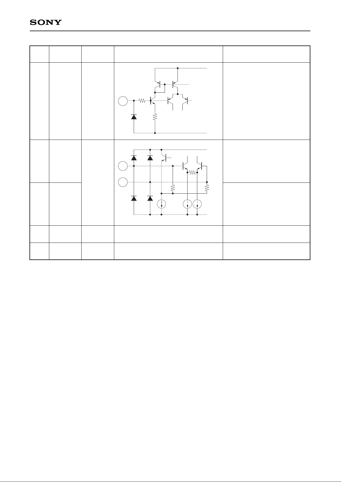
PS
IFINX
IFIN
VCC
GND
—
1.25 V
—
—
Power saving control.
IF inverted signal input.
IF signal input.
Power supply.
Ground.
VCC
GND
11
40k
60k
VCC
GND
13
14
1.1k 1.1k
800
 Loading...