

Sony CXA3125N Datasheet

—1—
E97705A85-TE
Sony reserves the right to change products and specifications without prior notice. This information does not convey any license by
any implication or otherwise under any patents or other right. Application circuits shown, if any, are typical examples illustrating the
operation of the devices. Sony cannot assume responsibility for any problems arising out of the use of these circuits.
Absolute Maximum Ratings (Ta=25 °C)
• Supply voltage VCC –0.3 to +5.5 V
• Storage temperature Tstg –55 to +150 °C
• Allowable power dissipation
PD 625 mW
(when mounted on a printed circuit board)
Operating Conditions
• Supply voltage VCC 4.75 to 5.30 V
• Operating temperature Topr –20 to +75 °C
Description
The CXA3125N is a TV tuner IC which integrates
local oscillator and mixer circuits for VHF band, local
oscillator and mixer circuits for UHF band, and an IF
amplifier onto a single chip. This IC adopts a 16-pin
SSOP package and is suitable for miniaturizing
voltage synthesizer tuner.
Features
• Low noise figure
• Superior cross modulation
• Low power consumption (5 V, 43 mA typ.)
• IF output can be selected from symmetrical or
asymmetrical
• SSOP 16-pin package
Applications
• TV tuners
• VCR tuners
• CATV tuners
Structure
Bipolar silicon monolithic IC
All Band TV Tuner IC (VHF-CATV-UHF)
16 pin SSOP (Plastic)
CXA3125N
For the availability of this product, please contact the sales office.

—2—
CXA3125N
Block Diagram and Pin Configuration
CXA3125N
OUTPUT
Buffer
UHFOSC
IF AMP
UHFMIXVHFMIX
VHFOSC
IFout1
IFout2
UOSC2
BSW
UOSC1
VOSC2
IFSW
VOSC1
V
CC
MIXout1
MIXout2
GND
VHFin1
VHFin2
UHFin1
UHFin2
V.REG
Bias
1 2 6 7 83 4 5
15 14 12 11 10 916 13

—3—
CXA3125N
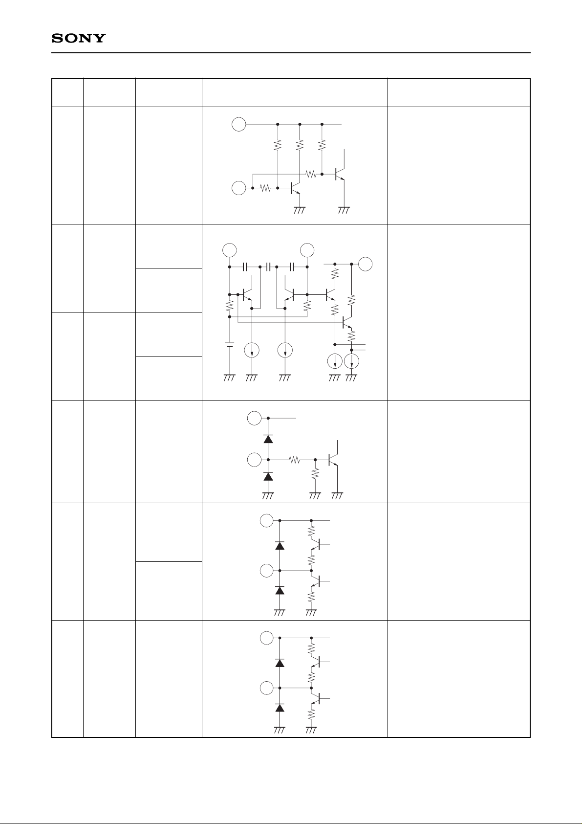
Pin Description and Equivalent Circuit
Pin
Symbol
Typical pin
Equivalent circuit Description
No. voltage (V)
1
2
3
4
5
6
7
8
9
11
VCC
MIXout1
MIXout2
GND
VHFin1
VHFin2
UHFin1
UHFin2
VOSC1
VOSC2
5.0
During VHF
reception 4.4
During UHF
reception 4.3
4.4
4.3
0
2.4
0
2.4
0
0
2.4
0
2.4
3.1
3.2
4.0
5.0
Power supply.
Mixer outputs and IF amplifier
inputs. These pins are output
with open collector, and they
must be connected to power
supply via load.
GND.
VHF inputs.
Normally a capacitor is
connected at Pin 5 to GND and
Pin 6 is used for input.
UHF inputs. Symmetrical input
to Pins 7 and 8 or a capacitor
is connected at Pin 8 to GND
and Pin 7 is used for input.
External resonance circuit
connection for VHF oscillators.
2 3
6
3k3k
5
8
3k3k
7
11
330
3k
8p
15p
3k
9
50
1
VCC
—4—
CXA3125N
Pin
Symbol
Typical pin
Equivalent circuit Description
No. voltage (V)
10
12
14
13
15
16
IFSW
UOSC1
UOSC2
BSW
IFout2
IFout1
0.8
(when open)
3.2
3.0
3.2
3.0
—
During
symmetrical
output 3.0
During
asymmetrical
output 4.3
During
symmetrical
output 3.0
During
asymmetrical
output 2.5
Symmetrical/asymmetrical
selection of IF output.
Asymmetrical output is selected
for open state; symmetrical
output, for connecting to GND.
When used as an asymmetrical
output, connect to GND with a
capacitor.
External resonance circuit
connection for UHF oscillators.
Band switching.
UHF operation when 3 V or
more voltage is applied
externally, and VHF operation
when 0.5 V or less voltage is
applied.
IF outputs during symmetrical
output. The reverse phase
signal to Pin 16 is output
during symmetrical output.
When asymmetrical output is
selected, the signal is not
output.
IF outputs.
3k 3k
1
VCC
1214
VCC
1
13
22k
32k
40k
VCC
1
30k
10
400
20k
400
30k
VCC
1
15
15
VCC
1
16
15
 Loading...