

Sony CXA3117AN Datasheet
– 1 –
CXA3117AN
E97220A8Z
IF Amplifier for M-ary FSK Pagers
Description
The CXA3117AN is a low current consumption FM
IF amplifier which employs the newest bipolar
process. It is suitable for M-ary FSK pagers.
Features
• Low current consumption: 1.1mA
(typ. at VCC = 1.4V)
• Low voltage operation: VCC = 1.1 to 4.0V
• Small package 24-pin SSOP
• Second mixer and oscillator
• Needless of IF decoupling capacitor
• Reference power supply for operational amplifier
and comparator
• Bit rate filter with variable cut-off
• Misoperation prevention function for continuous data
• RSSI function
• IF input, VCC standard
• Quick charge by the detector output sense method
Applications
• M-ary FSK pagers
• Double conversion pagers
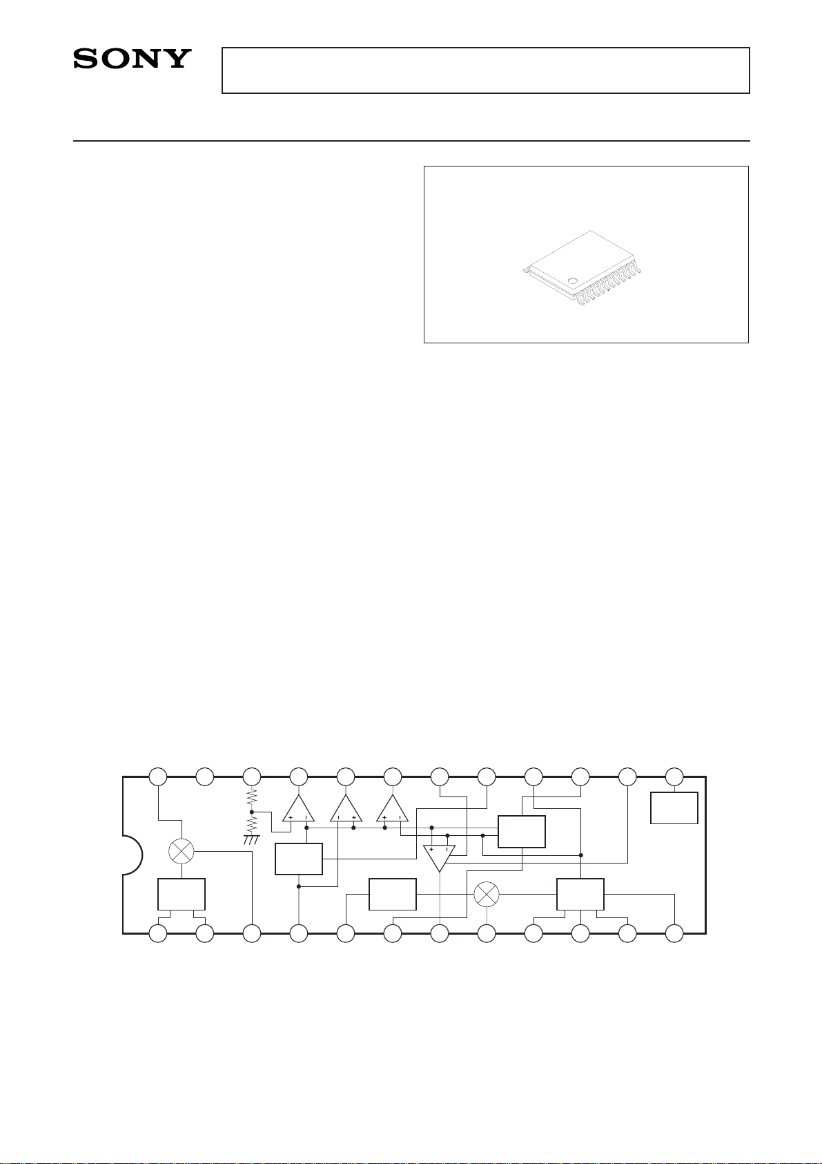
Block Diagram and Pin Configuration
Structure
Bipolar silicon monolithic IC
Absolute Maximum Ratings
• Supply voltage VCC 7.0 V
• Operating temperature Topr –20 to +75 °C
• Storage temperature Tstg –65 to +150 °C
• Allowable power dissipation PD 417 mW
Operating Condition
Supply voltage VCC 1.1 to 4.0 V
Sony reserves the right to change products and specifications without prior notice. This information does not convey any license by
any implication or otherwise under any patents or other right. Application circuits shown, if any, are typical examples illustrating the
operation of the devices. Sony cannot assume responsibility for any problems arising out of the use of these circuits.
24 pin SSOP (Plastic)
MIX IN
GND
REG OUT
REG CONT
LVA OUT
NRZ OUT
CHARGE
B.S.
AUDIO
L.C. OUT
CHG OFF
RSSI
OSC IN
OSC OUT
MIX OUT
V
CC
IF IN
TH CONT
FSK REF
QUAD
C1
C2
C3
FIL SW
OSC IF_LIM FILTER
MIX
QUAD_DET
LEVEL
COMP
REG
RSSI
CHARGE
GND
LVA
13
14
15
16
17
18
19
20
21
22
23
24
2
3
4
5
6
7
8
9
10
11
12
1
– 2 –
CXA3117AN
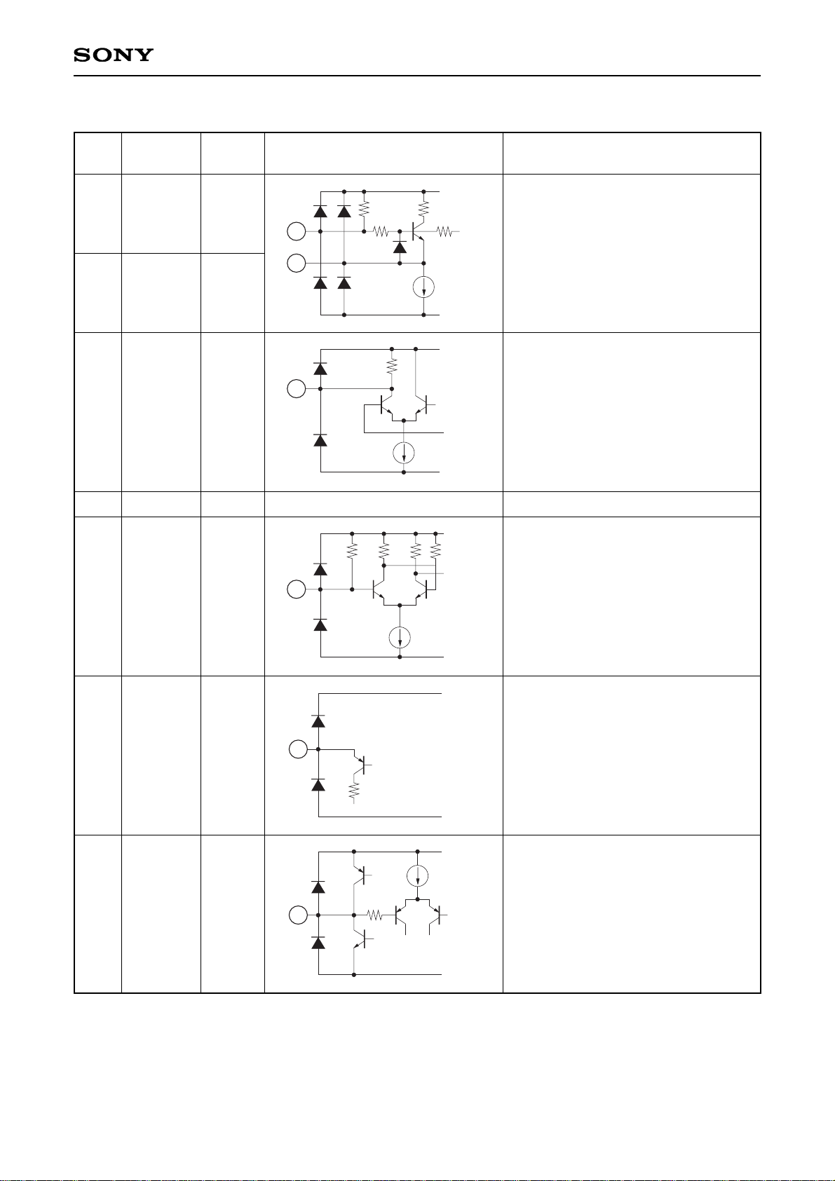
Pin Description
Pin
No.
1 1.4V
0.7V
1.3V
1.4V
—
0.2V
OSC IN
Connects the external parts of crystal
oscillator circuit.
A capacitor and crystal oscillator are
connected to these pins and VCC.
Mixer output.
Connect a 455kHz ceramic filter
between this pin and IF IN.
IF limiter amplifier input.
Determines the level comparator
threshold value.
Threshold value can be adjusted by
inserting the resistor between Pin 6 and
VCC.
Normally, short to VCC.
Connects the capacitor that determines
the low cut-off frequency for the entire
system.
Power supply.
OSC OUT
MIX OUT
VCC
IF IN
TH CONT
FSK REF
2
3
4
5
6
7
Symbol
Pin
voltage
Equivalent circuit Description
2
1
GND
VCC
300
15k
15k
72
GND
VCC
3
1.5k
GND
VCC
20k
5
1.5k
1.5k 20k
GND
VCC
6
25k
GND
VCC
72
7

– 3 –
CXA3117AN
Pin
No.
8
1.4VQUAD
9
10
11
0.2V
C1
C2
C3
12 —FIL SW
13 0.1VRSSI
14 —CHG OFF
Connects the phase shifter of FM
detector circuit.
Connects the capacitor that determines
the LPF cut-off.
Switches the LPF cut-off.
Cut-off is decreased by setting this pin
high.
(Applied voltage range: –0.5V to +7.0V)
RSSI circuit output.
Sets off the quick charge circuit
current. The charge current is off by
setting Pin 18 low and Pin 14 high.
Symbol
Pin
voltage
Equivalent circuit Description
8
GND
VCC
22k20k
20p
GND
VCC
9
10
11
35k
50k
GND
140k
20k
72
12
GND
VCC
7k 7k
13
70k
GND
100k
20k
72
14

– 4 –
CXA3117AN
Pin
No.
15
19
20
—
—
—
L.C. OUT
NRZ OUT
LVA OUT
Level comparator, NRZ comparator
and LVA comparator outputs. They are
open collectors.
(Applied voltage range: –0.5V to +7.0V)
18 —CHARGE
Controls the speed of the quick charge
circuit. Set this pin high to execute the
quick charge.
(Applied voltage range: –0.5V to +7.0V)
21 —
REG
CONT
Output for internal constant-voltage
source amplifier. Connect the base of
PNP transistor.
(Current capacity: 100µA)
22 1.0VREG OUT
Constant-voltage source output.
Controlled to maintain 1.0V.
23 —GND Ground
17—B.S.
Controls the battery saving.
Setting this pin low suspends the
operation of IC.
(Applied voltage range: –0.5V to +7.0V)
Symbol
Pin
voltage
Equivalent circuit Description
GND
72
15
19
20
GND
140k
20k
72
17
16
0.2V
AUDIO
Level comparator and NRZ comparator
inputs. The filter circuit output is
connected.
GND
VCC
72
16
72
GND
100k
20k
18
GND
VCC
72
21
GND
VCC
78k
22
22k
1k

– 5 –
CXA3117AN
Pin
No.
24 1.4VMIX IN Mixer input.
Symbol
Pin
voltage
Equivalent circuit Description
GND
VCC
4.16k
2k
4.16k
24
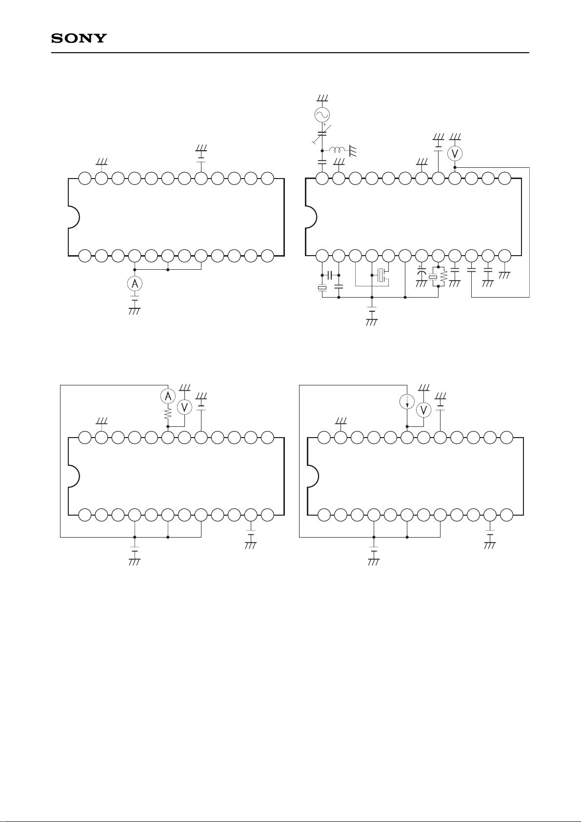
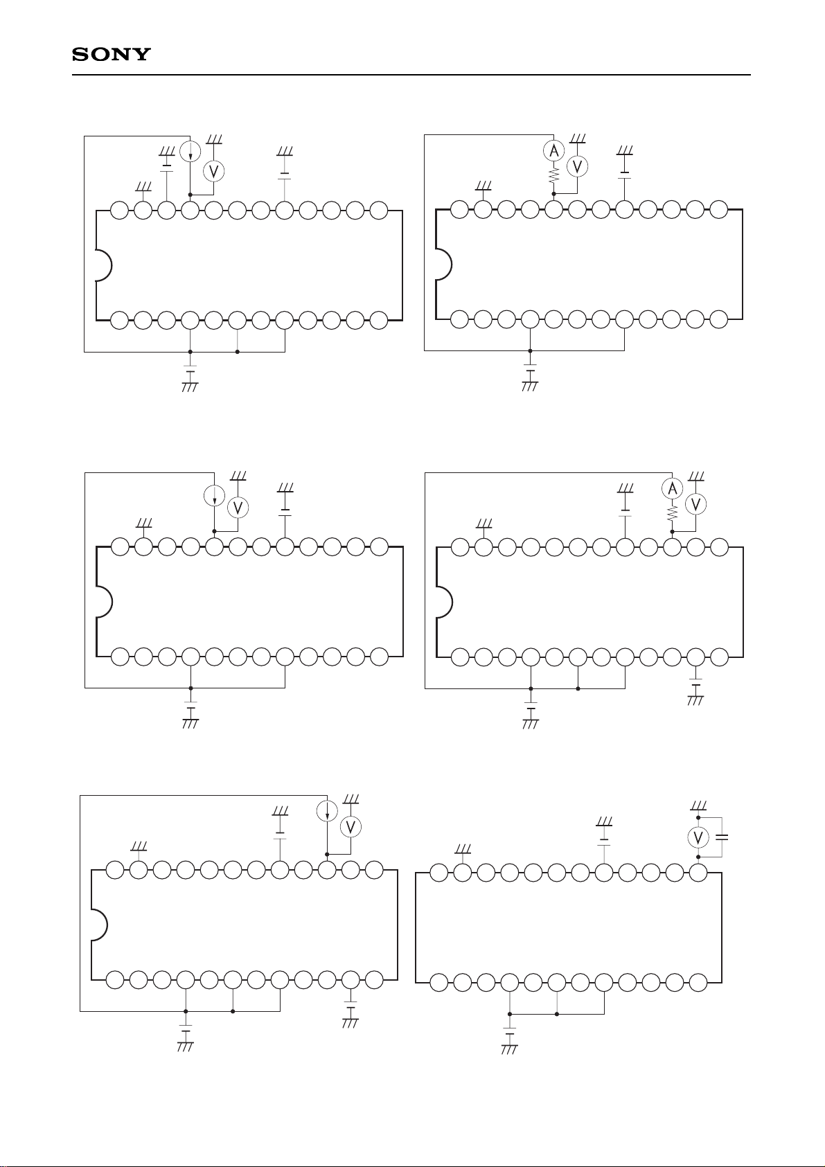
Electrical Characteristics
(VCC = 1.4V, Ta = 25°C, Fs = 21.7MHz, FMOD = 1.6kHz, FDEV = 4.8kHz, AMMOD = 30%)
Item
Current consumption
Current consumption
AM rejection ratio
NRZ output saturation voltage
NRZ output leak current
NRZ hysteresis width
VB output current
VB output saturation voltage
REG OUT voltage
LVA operating voltage
LVA output leak current
LVA output saturation voltage
Detector output voltage
Logic input voltage high level
Logic input voltage low level
Limiting sensitivity
Detector output level ratio
deviation to level comparator
window width
Level comparator output
saturation voltage
Level comparator output leak
current
RSSI output offset
Mixer input resistance
Mixer output resistance
IF limiter input resistance
ICC
ICCS
AMRR
VSATNRZ
ILNRZ
VTWNRZ
IOUT
VSATVB
VREG
VLVA
ILLVA
VSATLVA
VODET
VTHBSV
VTLBSV
VIN (LIM)
VLCWR
VSATLC
ILLC
VORSSI
RINLIM
ROUTMIX
RINLIM
Measurement circuit 1, V2 = 1.0V
Measurement circuit 1, V2 = 0V
Measurement circuit 2, 30k LPF
Measurement circuit 4, Vin = 0.3V
Measurement circuit 3, Vin = 0.1V
Measurement circuit 3,
Vin = 0.1 to 0.3V
Measurement circuit 5
Measurement circuit 5
Output current 0µA
Measurement circuit 6,
V1 = 1.4 to 1.0V
Measurement circuit 6, V1 = 1.0V
Measurement circuit 7
Measurement circuit 2
—
—
Measurement circuit 2,
Data filter fc = 2.4kHz
When Pin 6 is shorted to Vcc
Measurement circuit 9
Measurement circuit 8
Measurement circuit 10
—
—
—
0.7
—
25
—
—
0
100
—
0.95
1.05
—
—
50
0.9
—
—
–15
—
—
—
1.6
1.2
1.2
1.1
6
—
—
—
10
—
—
1.00
1.10
—
—
63
—
—
–108
0
—
—
150
2.0
1.5
1.5
1.35
10
—
0.4
5.0
20
—
0.4
1.05
1.15
5.0
0.4
80
—
0.35
—
+15
0.4
5.0
300
2.4
1.8
1.8
mA
µA
dB
V
µA
mV
µA
V
V
V
µA
V
mVrms
V
V
dBm
%
V
µA
mV
kΩ
kΩ
kΩ
Symbol Conditions Min. Typ. Max. Unit
– 6 –
CXA3117AN
V2
V1
1.4V
2
3
4
5
6
7
9
10
11
12
1
13
14
15
16
17
18
20
21
22
23
24
VCC
8
19
1000p
1.8µ
10p to
120p
Vin
V2
1V
1200p
1200p
8.2k
1200p
1µ
V1
1.4V
22p
2
3
4
5
6
7
8
9
10
11
12
1
13
14
15
16
17
18
19
20
21
22
23
24
15p
V
CC
Measurement circuit 1 Measurement circuit 2
V2
1V
V1
1.4V
2
3
4
5
6
7
9
10
11
12
1
13
14
15
16
17
18
20
21
22
23
24
VCC
Vin
8
19
100k
V2
1V
V1
1.4V
2
3
4
5
6
7
9
10
11
12
1
13
14
15
16
17
18
20
21
22
23
24
VCC
Vin
8
19
50µA
Measurement circuit 3 Measurement circuit 4
Electrical Characteristics Measurement Circuit
– 7 –
CXA3117AN
V3
0.5V
V2
1V
V1
1.4V
2
3
4
5
6
7
9
10
11
12
1
13
14
15
16
17
18
22
23
24
VCC
19
100µA
20
8
GND
GND
21
V2
1V
V1
1.4 to 1.0V
2
3
4
5
6
7
9
10
11
12
1
13
14
15
16
17
18
21
22
23
24
VCC
19
100k
20
8
Measurement circuit 5 Measurement circuit 6
V2
1V
V1
1.4V
2
3
4
5
6
7
9
10
11
12
1
13
14
15
16
17
18
21
22
23
24
VCC
19
50µA
20
8
Vin
0.2V
V2
1V
V1
1.4V
2
3
4
5
6
7
9
10
11
12
1
13
14
16
17
18
21
22
23
24
VCC
19
20
8
15
100k
Measurement circuit 7 Measurement circuit 8
Vin
0.1V
V2
1V
V1
1.4V
2
3
4
5
6
7
9
10
11
12
1
13
14
16
17
18
21
22
23
24
VCC
19
20
8
15
50µA
V2
1V
V1
1.4V
2
3
4
5
6
7
9
10
11
12
1
14
15
16
17
18
20
21
22
23
24
V
CC
8
19
13
100P
Measurement circuit 9 Measurement circuit 10
– 8 –
CXA3117AN
OSC IF_LIM FILTER
MIX
QUAD_DET
LEVEL
COMP
REG
RSSI
CHARGE
GND
LVA
VB_
REG
NRZ_
COMP
CHARGE BS AUDIO L.C.
OUT
CHG_
OFF
FIL_SW
VCC
GND
2
3
4
5
6
7
8
9
10
11
12
1
13
14
15
16
17
18
19
20
21
22
23
24
AUDIO
RSSI
LEVEL
NRZ
LVA
REG
GND
GND
C1
10p to 120p
L1
1.8µH
C3
1000p
GND
C6
10µ
GND
PNP
R4
220
C9
0.01µ
GND
R5
100k
R6
100k
GND GND GND
S4 S3
R8
100k
S2
GND
C14
100p
GND
S1
C13
1420p
(1200p + 220p)
R7
6.8k
GND
C12
680p
C11
1100p
(100p +
1000p)
GND
DISC
GND
C10
1µ
CERAFIL
C8
0.01µ
C7
10µ
GND
C5
15p
C4
22p
XTAL
RF
SMA
Application circuit
Application circuits shown are typical examples illustrating the operation of the devices. Sony cannot assume responsibility for
any problems arising out of the use of these circuits or for any infringement of third party patent and other right due to same.
– 9 –
CXA3117AN
Application Note
1) Power Supply
The CXA3117AN, with the built-in regulator, is designed to permit stable operation at the wide range of
supply voltage from 1.1 to 4.0V. Decouple the wiring to VCC (Pin 4) as close to the pin as possible.
2) Oscillator Input
Oscillator input method
a) Using Pins 1 and 2, input self-excited oscillation signal through the composition of a Colpitts type crystal
oscillator circuit. Connect the capacitors attached to the crystal and Pin 2 to VCC.
b) Directly input a local oscillation signal to Pin 1.
2
3
1
V
CC
Ceramic
filter
2
3
1
From
local signal
Ceramic
filter
Fig. 1
3) Mixer
The mixer is of double-balance type. Pin 24 is the input pin. Input though a suitable matching circuit. The
input impedance is 2.0kΩ.
Pin 3 serves as the output pin for the mixer, and a load resistance of 1.5kΩ is incorporated.
4) IF Filter
The filter to be connected between this mixer output and the IF limiter amplifier input should have the
following specifications. Connect the ground pin of the IF filter to VCC.
I/O impedance : 1.5kΩ ±10%
Bandwidth : Changes according to applications.
5) IF Limiter Amplifier
The gain of this IF limiter amplifier is approximately 100dB. Take notice of the following points in making
connection to the IF limiter amplifier input pin (Pin 5).
a) Wiring to the IF limiter amplifier input (Pin 5) should be as short as possible.
b) As the IF limiter amplifier output appears at QUAD (Pin 8), wiring to the ceramic discriminator connected
to QUAD should be as short as possible to reduce the interference with the mixer output and IF limiter
amplifier input.
VCC
Wire as short and apart as possible As short as possible
3
4
5
6
7
8
9
Fig. 2
 Loading...