

Sony CXA3108AQ Datasheet

—1—
E99904-TE
Sony reserves the right to change products and specifications without prior notice. This information does not convey any license by
any implication or otherwise under any patents or other right. Application circuits shown, if any, are typical examples illustrating the
operation of the devices. Sony cannot assume responsibility for any problems arising out of the use of these circuits.
Absolute Maximum Ratings (Ta=25 °C)
• Supply voltage VCC –0.3 to +5.5 V
• Storage temperature Tstg –55 to +150 °C
• Allowable power dissipation
PD 730 mW
(when mounted on a substrate)
Operating Conditions
• Supply voltage VCC 4.75 to 5.30 V
• Operating temperature Topr –25 to +75 °C
Description
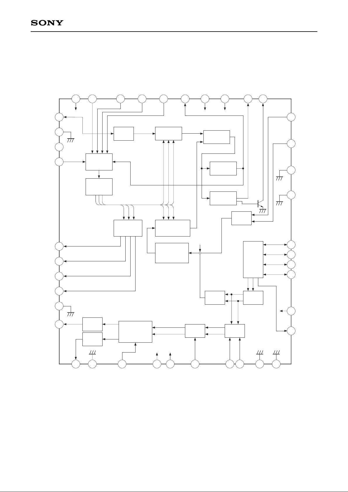
The CXA3108AQ is a monolithic IC that downconverts the L-band (1 to 2 GHz) 1st IF to 2nd IF for
satellite broadcast receivers. It integrates a local
oscillator circuit, double-balanced mixer, IF AGC
amplifier and tuning PLL onto a single chip.
This IC supports both analog and digital satellite
broadcasts, and achieves reduction in the number of
tuner components and smaller size.
Features
• On-chip tuning PLL
• Supports 2.65 GHz oscillator frequency
• Noise figure: 12.5 dB typ. (for IF full gain)
• IF AGC gain variation: 46 dB typ.
• Wide band IF AGC amplifier (60 to 500 MHz)
• Two IF outputs
• PLL supports I2C protocol
• On-chip high voltage drive transistor for charge
pump
Applications
• Analog satellite broadcast tuners (BS/CS)
• Digital satellite broadcast tuners (DSS/DVB, etc.)
Structure
Bipolar silicon monolithic IC
L-band Down Converter IC with On-Chip PLL
40 pin QFP (Plastic)
CXA3108AQ
Notes on Handling
This IC has a weak electrostatic discharge strength. Take care when handling the IC.
—2—
CXA3108AQ
Block Diagram and Pin Configuration
21
36
37
38
40
I2C
Receiver
30 29
31
32
35
34
33
Divider
11bit
Phase
Detector
28 27 26 25 22
Shift
Register
39
1
24 23
Lock
Det
Charge
Pump
Buffer
20
19
Divider
17 bit
Prescaler
1/2, 1/1
STSW
Buffer Buffer
16
15
14
13
OSC
18
17
11MIX
87
10
9
IF AGC
AMP
654
IF VCC
SAW
Driver
SAW
Driver
2
OUTPUT SW
3
XTAL
DGND1
NC
BUSSW
PS1
PS2
PS3
PS4
GND
IFOUT2
DV
CC
1
ADSW
SCL
SDA
ADC
LOCK
DV
CC
2
STSW
CPO
VT
IFOUT1
IFGND2
IFSW
IFV
CC
2
IFV
CC
1
IFAGC
RFIN1
RFIN2
IFGND1
RFGND
EXTIN2
EXTIN1
DGND2
GND
OSCB2
OSCE2
OSCE1
OSCB1
RFV
CC
BIAS
REF
OSC
Output Port
Driver
12
—3—
CXA3108AQ
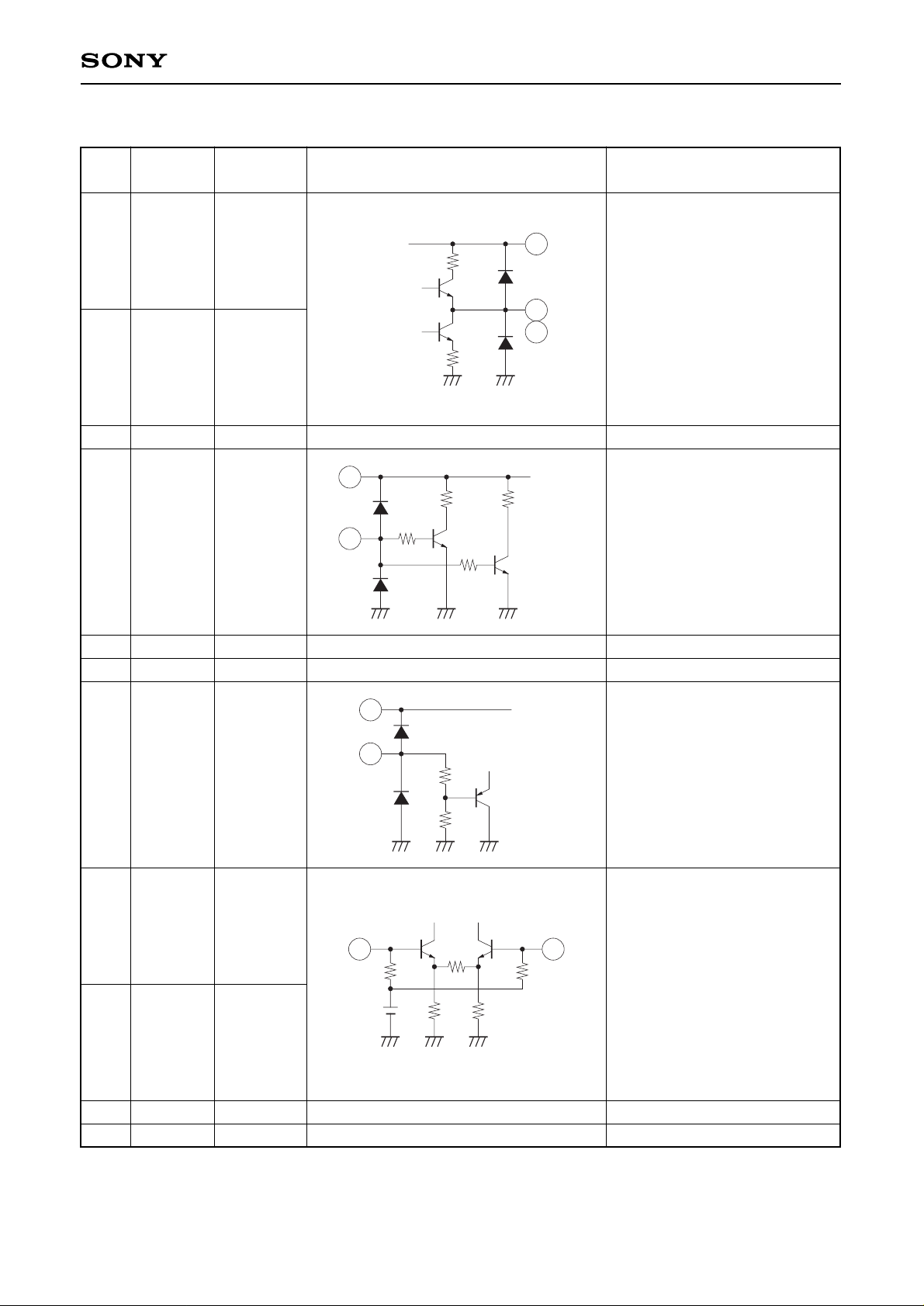
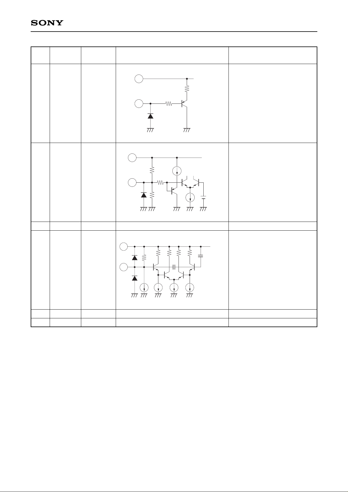
Pin Description
Pin
Symbol
Pin voltage
Equivalent circuit Description
No. [V]
1
40
2
3
4
5
6
7
8
9
10
IFOUT1
IFOUT2
IFGND2
IFSW
IFVCC2
IFVCC1
IFAGC
RFIN1
RFIN2
IFGND1
RFGND
2.5
(IFSW 0 V)
4.7
(IFSW 5 V)
4.7
(IFSW 0 V)
2.5
(IFSW 5 V)
0
0 or 5
5
5
0 to 4
1.7
1.7
0
0
IF outputs.
IF output circuit GND.
Selects whether IF output is
Pin 1 or Pin 40.
When this pin is connected to
GND, the IF signal is output
from Pin 1; when connected to
VCC, the IF signal is output from
Pin 40.
IF output circuit power supply.
IF amplifier circuit power supply.
AGC signal input.
RF inputs.
IF amplifier circuit GND.
RF block GND.
IFVCC2
4
1
40
IFVCC2
4
3
30k
100k
IFVCC1
40k
5
40k
6
7 8
2k 2k
—4—
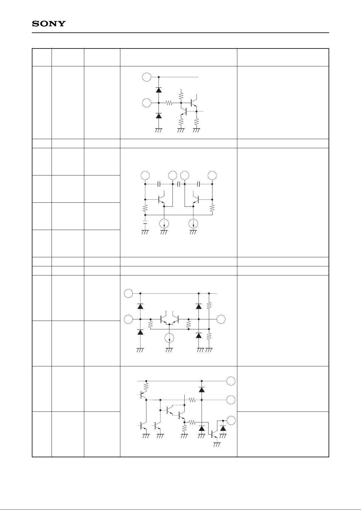
CXA3108AQ
Pin
Symbol
Pin voltage
Equivalent circuit Description
No. [V]
11
12
13
14
15
16
17
18
19
20
21
22
BIAS
RFVCC
OSCB1
OSCE1
OSCE2
OSCB2
GND
DGND2
EXTIN1
EXTIN2
VT
CPO
1.8
5
2.2
1.5
1.5
2.2
0
0
2.5
2.5
—
—
Oscillator circuit current
adjustment.
Connect this pin to GND via a
capacitor.
RF block power supply.
Oscillator pins.
GND.
Charge pump GND.
PLL external inputs.
NPN transistor output for
varicap diode drive.
Charge pump output.
Connect a loop filter.
RFVCC
12
11
200
13
2.5k
14 15 16
2.5k
DVCC1
30
19
20k
20
25k
25k
5k
5k
DVCC2
24
22
200
500
20k
21
—5—
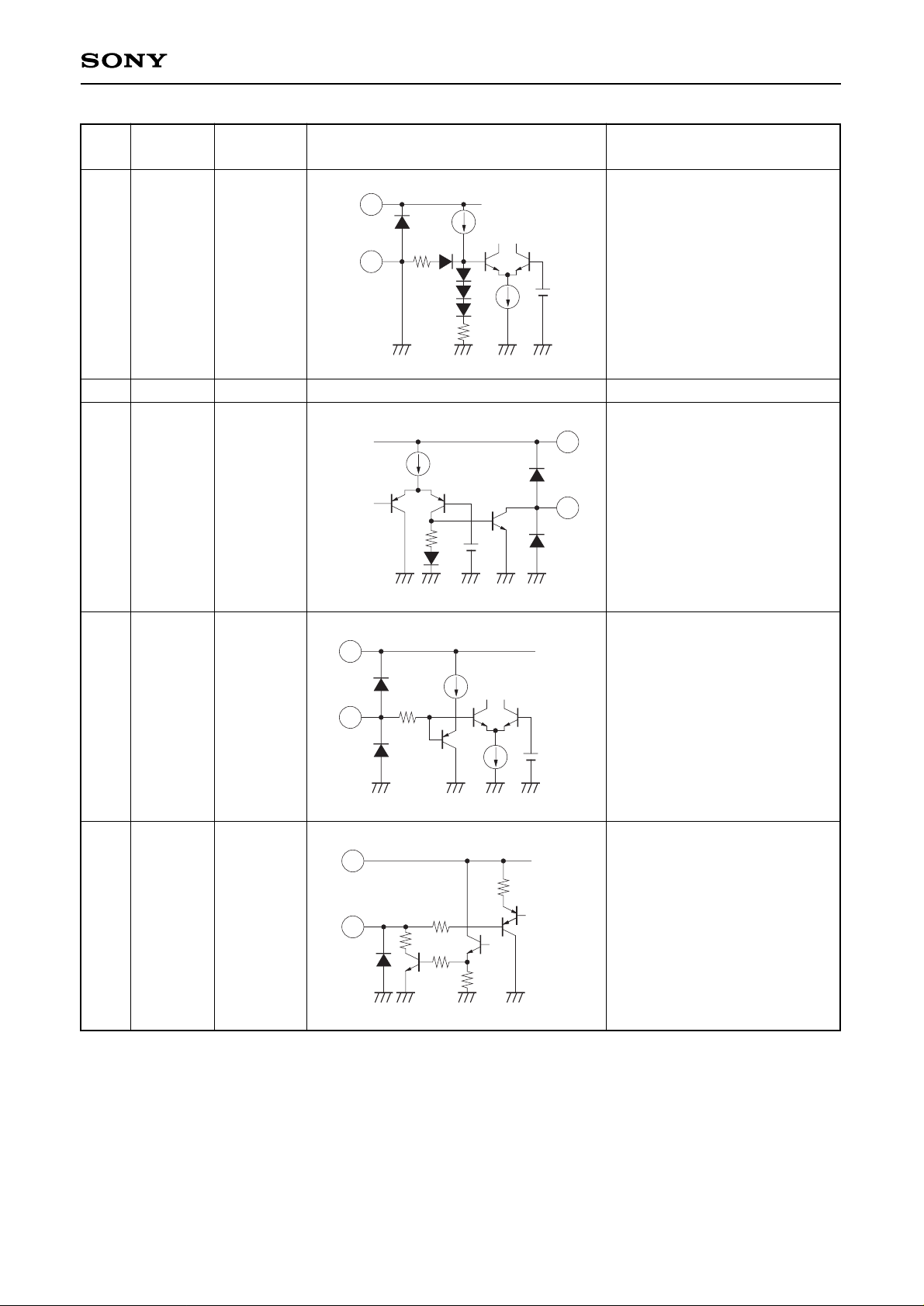
CXA3108AQ
Pin
Symbol
Pin voltage
Equivalent circuit Description
No. [V]
23
24
25
26
27
STSW
DVCC2
LOCK
ADC
SDA
—
5
5.0
(LOCK)
0.2
(UNLOCK)
—
—
Selects either the internal
oscillator circuit or external input
for input to PLL.
When this pin is open or
connected to VCC, the internal
oscillator circuit is selected;
when connected to GND,
external input is selected.
Charge pump power supply.
LOCK detection.
High when locked, Low when
unlocked.
ADC input.
DATA input.
DVCC1
20k
30
23
DVCC1
30
25
DVCC1
30
26
DVCC1
30
27
5k
20
2.5k
40k
—6—
CXA3108AQ
Pin
Symbol
Pin voltage
Equivalent circuit Description
No. [V]
28
29
30
31
32
33
SCL
ADSW
DVCC1
XTAL
DGND1
NC
—
1.3
5
4.4
0
—
CLOCK input.
I2C bus address selection.
PLL circuit power supply.
Crystal connection for reference
oscillator.
PLL circuit GND.
DVCC1
30
28
DVCC1
30
29
150k
50k
60k
30p
30p
30
31
DVCC1
 Loading...