

Sony CXA3107N Datasheet

—1—
E96303A8Z
Sony reserves the right to change products and specifications without prior notice. This information does not convey any license by
any implication or otherwise under any patents or other right. Application circuits shown, if any, are typical examples illustrating the
operation of the devices. Sony cannot assume responsibility for any problems arising out of the use of these circuits.
Absolute Maximum Ratings (Ta=25 °C)
• Supply voltage VCC 7.0 V
• Operating temperature Topr –20 to +75 °C
• Storage temperature Tstg –65 to +150 °C
Operating Condition
Supply voltage VCC 1.1 to 4.0 V
Description
The CXA3107N is a low current consumption FM
IF amplifier which employs the newest bipolar
process. It is suitable for M-ary FSK pagers.
Features
• Low current consumption: 570 µA
(typ. at VCC=1.4 V)
• Low voltage operation: VCC=1.1 to 4.0 V
• Small package 20-pin SSOP
• Needless of IF decoupling capacitor
• Reference power supply for operational amplifier
and comparator
• Bit rate filter with variable cut-off
• Misoperation prevention function for continuous
data
• RSSI function
• IF input, Vcc standard
Applications
• M-ary FSK pagers
Function
Plastic
Structure
Bipolar silicon monolithic IC
IF Amplifier for M-ary FSK Pagers
20 pin SSOP (Plastic)
CXA3107N
For the availability of this product, please contact the sales office.
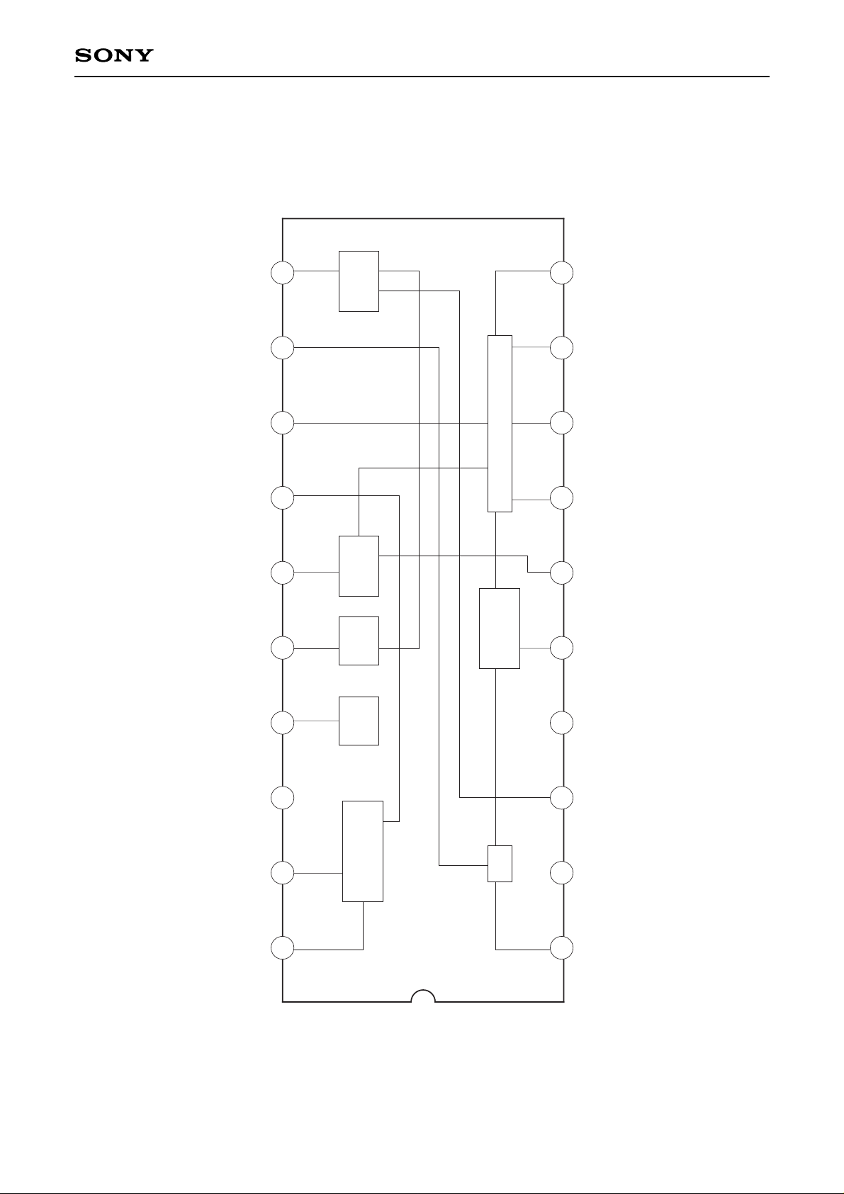
—2—
CXA3107N
VCC
REG
OUT
REG
CONT
CHARGE RSSI
DISKGNDIF IN
REGULATOR
LIM FILTER
QUAD
DET
QUICK
CHARGE
ALARM
LEVEL
COMP
111213141516171820 19
NRZ
COMP
LVA
NRZ
OUT
BS
FIL
SW
LEVEL
TH
CONT
FSK
REF
CHG
CONT
C1 C2 C3 AUDIO
1 2 3 4 5 6 7 8 9 10
Block Diagram
—3—
CXA3107N
Pin Description
Pin
Symbol Pin voltage Equivalent circuit Description
No.
1
2
3
4
5
6
IF IN
GND
TH CONT
FSK REF
DISK
CHG OFF
1.4 V
—
—
0.2 V
1.4 V
—
IF limiter amplifier input.
Ground.
Determines the level
comparator threshold value.
The threshold value can be
adjusted by inserting the
resistor between Pin 3 and
VCC.
Normally, short to VCC.
Connects the capacitor that
determines the low cut-off
frequency for the entire
system.
Connects the phase shifter of
FM detector circuit.
Sets off the quick charge
circuit current. The charge
current is off by setting Pin 15
low and Pin 6 high.
VCC
1.5k
GND
1.5k
20k 20k
1
VCC
GND
3
25k
VCC
GND
72
4
VCC
22k
GND
20p
20k
5
20k
GND
72k
6
100k
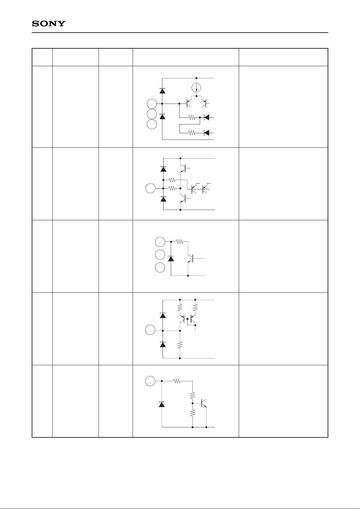
—4—
CXA3107N
Pin
Symbol Pin voltage Equivalent circuit Description
No.
7
8
9
10
11
16
17
12
13
C1
C2
C3
AUDIO
LEVEL
NRZ OUT
LVA OUT
RSSI
FIL SW
0.2 V
0.2 V
—
—
—
0.1 V
—
Connects the capacitor that
determines the LPF cut-off.
Level comparator and NRZ
comparator inputs.
The operational amplifier
output is connected.
Level comparator, NRZ
comparator and LVA
comparator outputs.
They are open collectors.
(Applied voltage range:
–0.5 V to +7.0 V)
RSSI circuit output.
Switches the LPF cut-off.
Cut-off is decreased by setting
this pin high.
(Applied voltage range:
–0.5 V to +7.0 V)
VCC
GND
35k
7
50k
8
9
VCC
GND
72
72
10
72
GND
11
16
17
VCC
GND
7k 7k
70k
12
20k
GND
72
13
140k
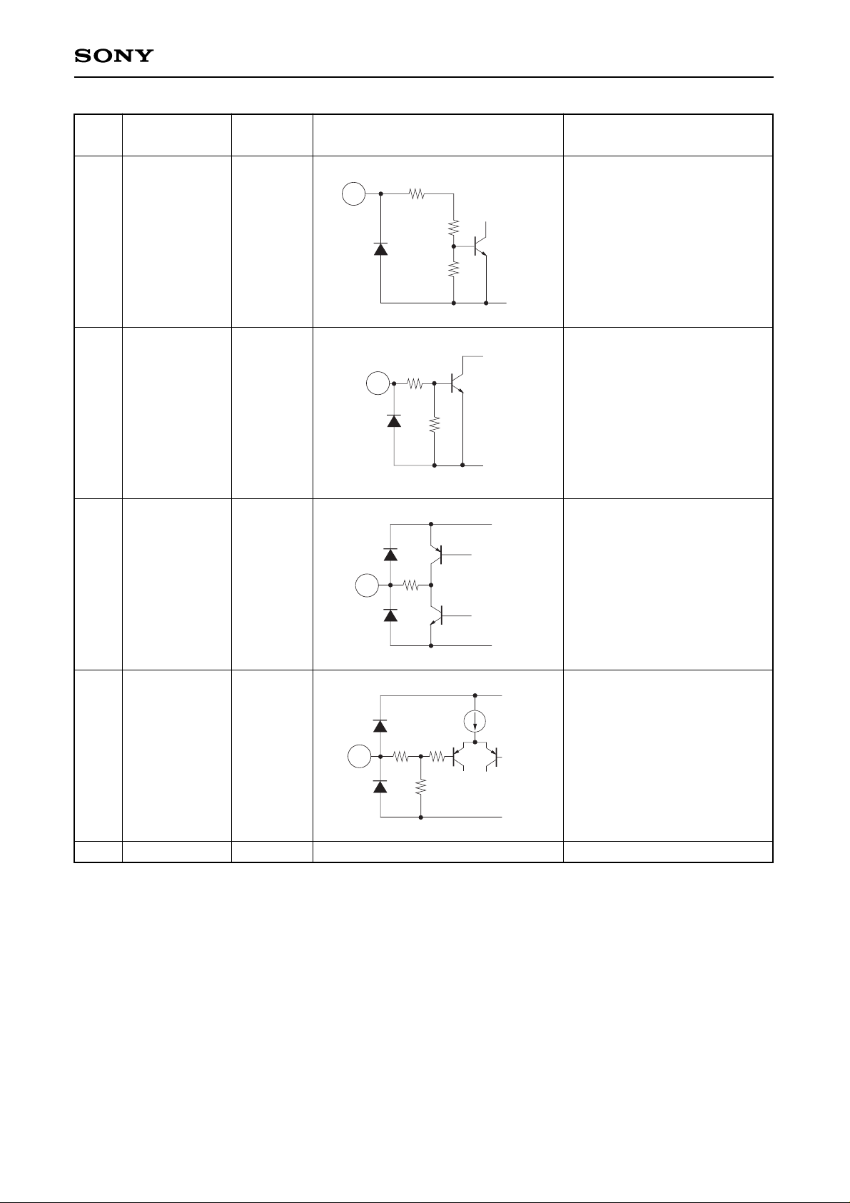
—5—
CXA3107N
Pin
Symbol Pin voltage Equivalent circuit Description
No.
14
15
18
19
20
B.S.
CHARGE
REG CONT
REG OUT
VCC
—
—
—
1.0 V
Controls the battery saving.
Setting this pin low suspends
the operation of IC.
(Applied voltage range:
–0.5 V to +7.0 V)
Controls the charge speed of
the quick charge circuit.
Set this pin high to execute the
quick charge.
(Applied voltage range:
–0.5 V to +7.0 V)
Output for internal constantvoltage source amplifier.
Connects the base of PNP
transistor.
(Current capacity: 100 µA)
Constant-voltage source
output.
Controlled to maintain 1.0 V.
Power supply.
20k
GND
72
14
140k
15
20k
100k
GND
18
VCC
GND
72
19
VCC
GND
78k
1k
22k
—6—
CXA3107N
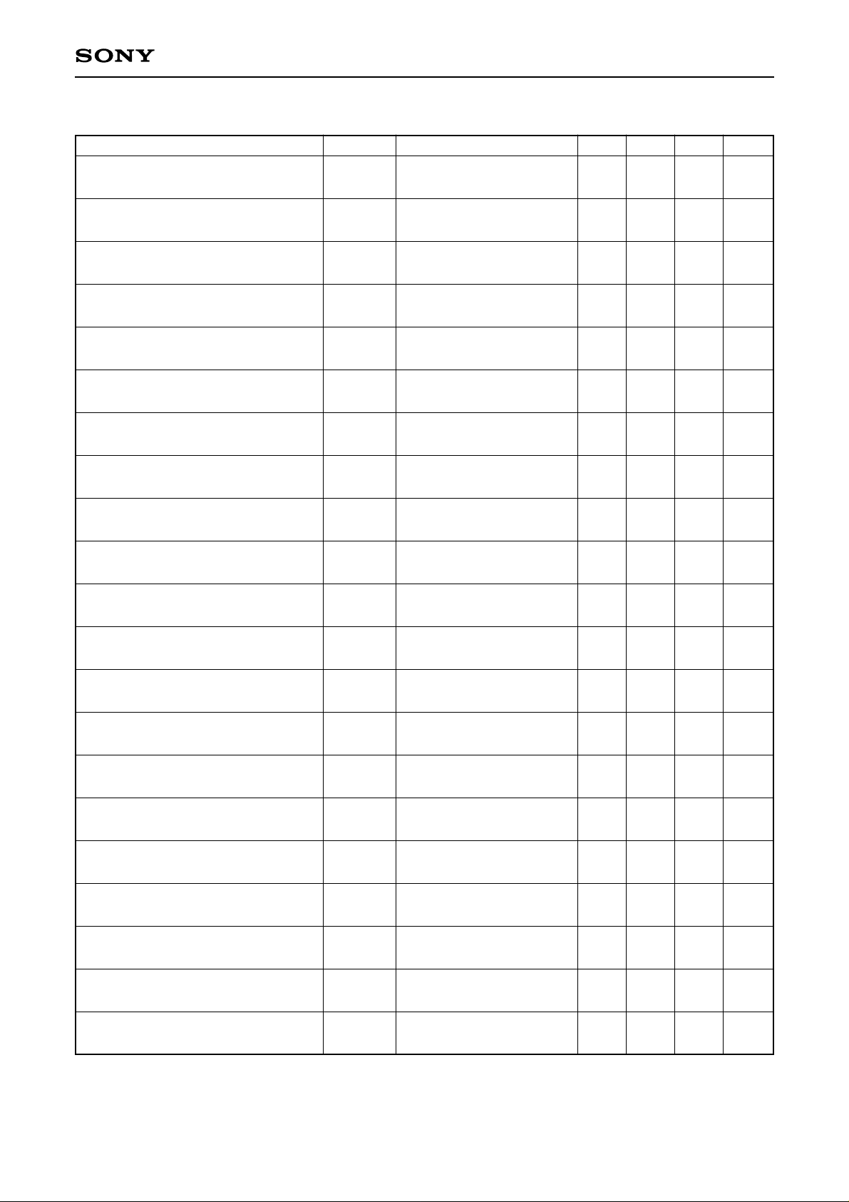
Electrical Characteristics (VCC=1.4 V, Ta=25 °C, FS=455 kHz, FMOD=1.6 kHz, FDEV=4.8 kHz, AMMOD=30 %)
Item
Current consumption
Current consumption
AM rejection ratio
NRZ output saturation voltage
NRZ output leak current
NRZ hysteresis width
VB output current
VB output saturation current
REG OUT voltage
LVA operating voltage
LVA output leak current
LVA output saturation voltage
Detector output voltage
Logic input voltage high level
Logic input voltage low level
Limiting sensitivity
Detector output level ratio deviation
to level comparator window width
Level comparator output saturation
voltage
Level comparator output leak current
RSSI output offset
IF limiter input resistance
Symbol
ICC
ICCS
AMRR
VSATNRZ
ILNRZ
VTWNRZ
IOUT
VSATVB
VREG
VLVA
ILLVA
VSATLVA
VODET
VTHBSV
VTLBSV
VIN (LIM)
VLCWR
VSATLC
ILLC
VORSSI
RINLIM
Conditions
Measurement circuit 1
V2=1.0 V
Measurement circuit 1
V2=0 V
Measurement circuit 2
30 k LPF
Measurement circuit 4
Vin=0.3 V
Measurement circuit 3
Vin=0.1 V
Measurement circuit 3
Vin=0.1 to 0.3 V
Measurement circuit 5
Measurement circuit 5
Output current 0 µA
Measurement circuit 6
V1=1.4 to 1.0 V
Measurement circuit 6
1=1.0 V
Measurement circuit 7
Measurement circuit 2
—
—
Measurement circuit 2,
data filter fc=2.4 kHz
—
Measurement circuit 9
Measurement circuit 8
Measurement circuit 10
—
Min. Typ. Max. Unit
390 570 780 µA
— 6 20 µA
25 — — dB
— — 0.4 V
— — 5.0 µA
5 10 20 mV
100 — — µA
— — 0.4 V
0.92 0.96 1.02 V
1.00 1.05 1.10 V
— — 5.0 µA
— — 0.4 V
50 63 80 mVrms
0.9 — — V
— — 0.35 V
— –83 — dBm
–15 0 +15 %
— — 0.4 V
— — 5.0 µA
— 100 250 mV
1.2 1.5 1.8 kΩ
 Loading...