

Sony CXA3106Q Datasheet
PLL IC for LCD Monitor/Projector
Description
The CXA3106Q is a PLL IC for LCD monitors/
projectors with built-in phase detector, charge pump,
VCO and counter.
The various internal settings are performed by
serial data via a 3-line bus.
Applicable LCD monitor/projector resolution are
VGA, SVGA and XGA, etc.
Features
• Supply voltage: 5V ± 10% single power supply
• Package: 48-pin QFP
• Power consumption: 335mW
• Sync input frequency: 10 to 100kHz
• Clock output signal frequency: 10 to 120MHz
• Clock delay: 1/16 to 20/16 CLK
• Sync delay: 1/16 to 20/16 CLK
• I/O level: TTL, PECL (complementary)
• Low clock jitter
• 1/2 clock output
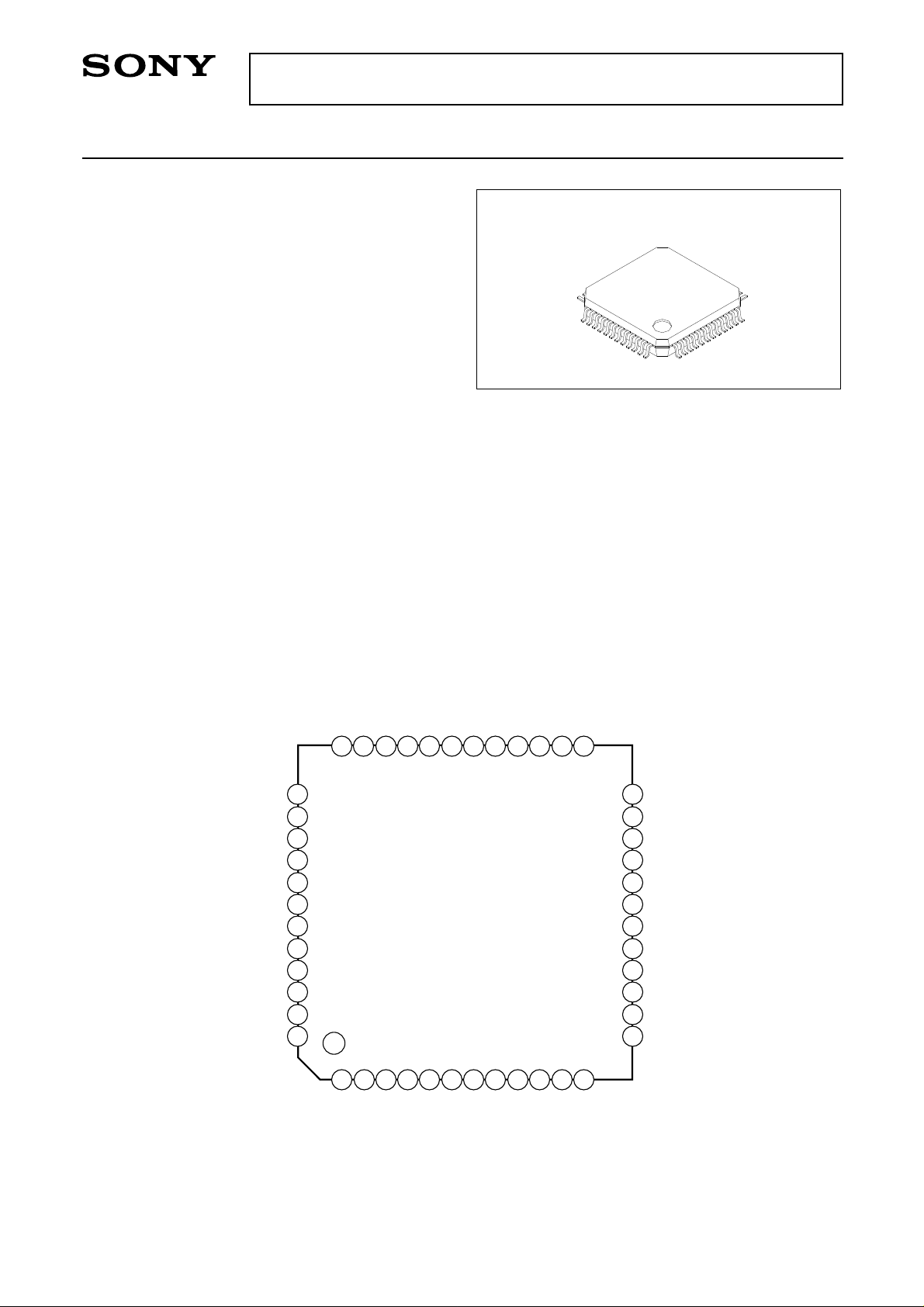
CXA3106Q
48 pin QFP (Plastic)
Functions
• Phase detector enable
• UNLOCK output
• Output TTL disable function
• Power save function (2 steps)
Applications
• CRT displays
• LCD projectors
• LCD monitors
• Multi-media
Pin Configuration (Top View)
IOGND
PLLV
PLLGND
VCOV
VCOGND
VCOHGND
IRGND
Sony reserves the right to change products and specifications without prior notice. This information does not convey any license by
any implication or otherwise under any patents or other right. Application circuits shown, if any, are typical examples illustrating the
operation of the devices. Sony cannot assume responsibility for any problems arising out of the use of these circuits.
IOVCC
CC
CC
IREF
RC2
RC1
IRVCC
37
38
39
40
41
42
43
44
45
46
47
48
CC
PECLV
36
1
CC
IOV
VBB
35
2
IOGND
DSYNCH
33
34
4
3
VCOH
CLKH
DSYNCL
32
31
6
5
VCO
VCOL
CLKL
30
7
HOLD
CLK/2L
CLK/2H
29
8
SYNCL
SYNCH
CC
PECLV
28
9
SYNC
IOGND
26
27
10
11
SENABLE
CC
TTLV
25
12
SCLK
TTLGND
23
20
19
18
17
16
15
14
13
SDATA
24
22
21
DSYNC
CLK
CLKN
CLK/2
CLK/2N
DGND
DV
CC
UNLOCK
DIVOUT
SEROUT
CS
TLOAD
– 1 –
E97447A7X-PS

CXA3106Q
Absolute Maximum Ratings (Ta = 25°C)
• Supply voltage IOVCC, DVCC, TTLVCC, PECLVCC, PLLVCC,
VCOVCC, IRVCC, –0.5 to +7.0 V
IOGND, DGND, TTLGND, VCOHGND, PLLGND,
VCOGND, IRGND –0.5 to +0.5 V
• Input voltage VCOH, VCOL, SYNCH, SYNCL, VCO, HOLD,
SYNC, SENABLE, SCLK, SDATA, TLOAD, CS IOGND – 0.5 to IOVCC + 0.5 V
RC2 IRGND – 0.5 to IRVCC + 0.5 V
• Output current SEROUT, DIVOUT, UNLOCK, CLK/2N, CLK/2,
CLKN, CLK, DSYNC, CLK/2L, CLK/2H, CLKL,
CLKH, DSYNCH, DSYNCL, VBB –30 to +30 mA
IREF, RC1 –2 to +2 mA
• Storage temperature Tstg –65 to +150 °C
• Operating ambient temperature
Ta –25 to +75 °C
• Allowable power dissipation
PD 750 mW
Recommended Operating Conditions
Min. Typ. Max.
• Supply voltage IOVCC, DVCC, TTLVCC, PECLVCC,
PLLVCC, VCOVCC, IRVCC 4.75 5.00 5.25 V
IOGND, DGND, TTLGND, VCOHGND,
PLLGND, VCOGND, IRGND –0.05 0 0.05 V
• Digital input DIN (PECL) ∗1H level IOVCC – 1.1
DIN (PECL) ∗1L level IOVCC – 1.5 V
DIN (TTL) ∗2H level 2.0 V
DIN (TTL) ∗2L level 0.8 V
• SYNC, SYNCH, SYNCL input jitter 1.0 ns
• Operating temperature
Ta –20 +75 °C
∗1
VCOH, VCOL, SYNCH, SYNCL
∗2
VCO, HOLD, SYNC, SENABLE, SCLK, SDATA, TLOAD, CS
– 2 –
DSYNC
(TTL)
DSYNC
(PECL)
CLK
(TTL)
NCLK
(TTL)
CLK
(PECL)
CLK/2
(TTL)
NCLK/2
(TTL)
CLK/2
(PECL)
UNLOCK
CXA3106Q
VBB
RC2RC1
1bit
on/off
1 to 4 CLK
TTLOUT
Polarity
Coarse
Delay
Latch
1bit
PECLOUT
on/off
1bit2bit
logic
1bit
TTLOUT
on/off
TTLOUT
PECLOUT
2bit
DIVMUXVCO
1bit5bit2bit
Fine
Delay
1/16 to 20/16 CLK
1/256 to 1/4096 CLK
1bit
TTLOUT
on/off
Programmable
Counter
1bit
on/off
12bit
TTLOUT
RSET
1/2
1bit
PECLOUT
on/off
unlock
detect
PECL
whole chip
power save
synthesizer
power save
TTLINTTLOUTCONTROL REGISTERDAC
1bit
on/off
CSTLOAD
1bit
DIVOUTSEROUT
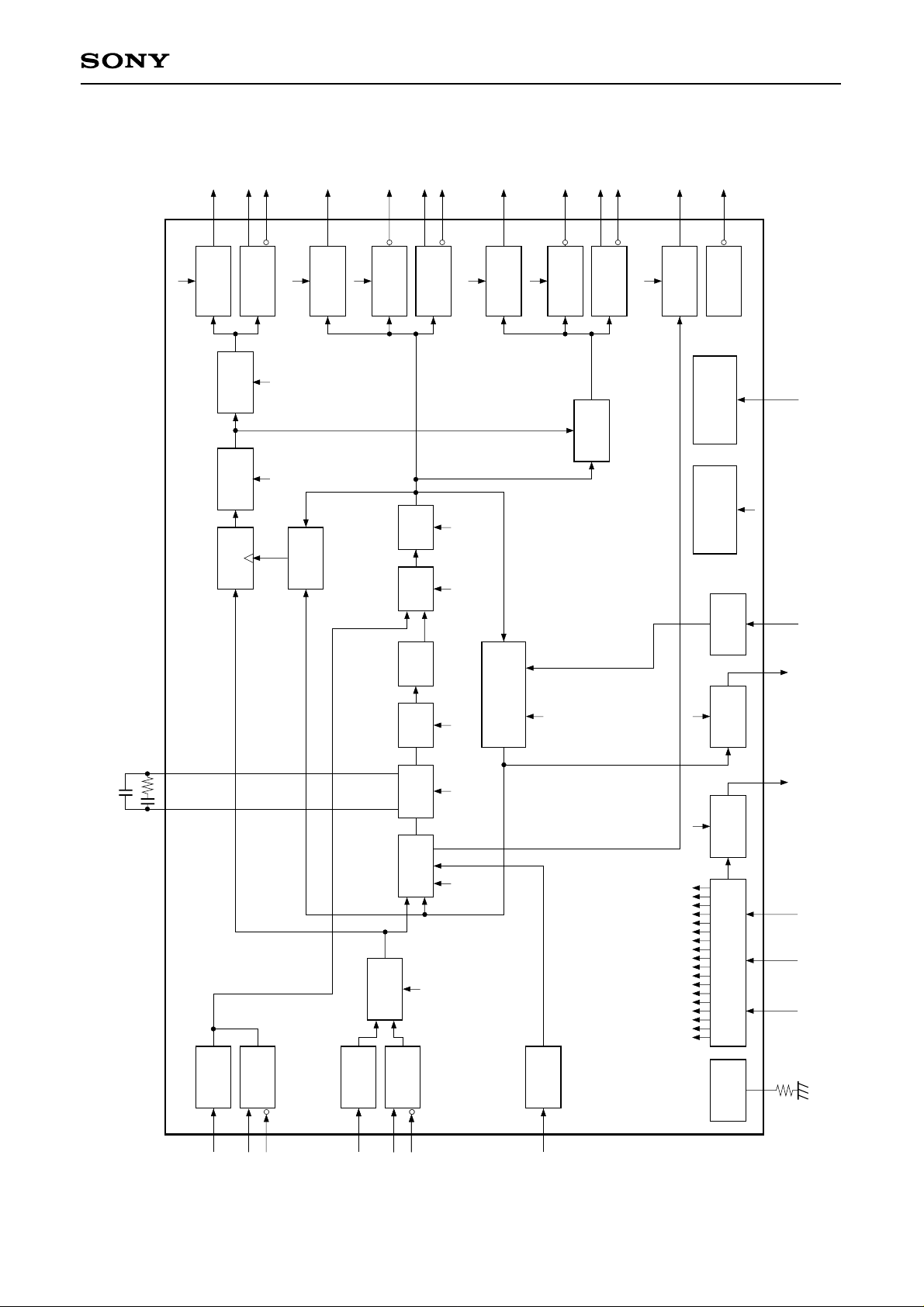
Block Diagram
TTLIN
VCO
(TTL)
PECLIN
VCO
(PECL)
TTLIN
SYNC
(TTL)
Charge
Phase
Polarity
PECLIN
SYNC
(PECL)
Pump
Detector
1bit
– 3 –
1bit
TTLIN
HOLD
(TTL)
1bit
on/off
read out
TTLOUT
SDATASCLKSENABLE
IREF

Pin No. Symbol Description Reference voltage level
1 IOVCC Digital power supply 5V
2 IOGND Digital GND 0V
3 VCOH External VCO input PECL
4 VCOL External inverted VCO input PECL
5 VCO External VCO input TTL
6 HOLD Phase detector disable signal input TTL
7 SYNCH Sync input PECL
8 SYNCL Inverted sync input PECL
9 SYNC Sync input TTL
10 SENABLE Control signal (enable) TTL
11 SCLK Control signal (clock) TTL
12 SDATA Control signal (data) TTL
13 TLOAD Programmable counter test input TTL
14 CS Chip select TTL
15 SEROUT Register read output TTL
16 DIVOUT Programmable counter test output TTL
17 UNLOCK Unlock signal output TTL
18 DVCC Digital power supply 5V
19 DGND Digital GND 0V
20 CLK/2N Inverted 1/2 clock output TTL
21 CLK/2 1/2 clock output TTL
22 CLKN Inverted clock output TTL
23 CLK Clock output TTL
24 DSYNC Delay sync signal output TTL
25 TTLGND TTL output GND 0V
26 TTLVCC TTL output power supply 5V
27 IOGND Digital GND 0V
28 PECLVCC PECL output power supply 5V
29 CLK/2L Inverted 1/2 clock output PECL
30 CLK/2H 1/2 clock output PECL
31 CLKL Inverted clock output PECL
32 CLKH Clock output PECL
33 DSYNCL Delay sync signal output PECL
34 DSYNCH Inverted delay sync signal output PECL
35 VBB PECL reference voltage PECLVCC – 1.3V
36 PECLVCC PECL output power supply 5V
37 IOGND Digital GND 0V
38 IOVCC Digital power supply 5V
39 PLLVCC PLL circuit analog power supply 5V
40 PLLGND PLL circuit analog GND 0V
41 VCOVCC VCO circuit analog power supply 5V
42 VCOGND VCO circuit analog GND 0V
43 VCOHGND VCO SUB analog GND 0V
44 IREF Charge pump current preparation 1.3V
45 RC2 External pin for LPF 2.0V to 4.4V
46 RC1 External pin for LPF 2.1V
47 IRGND IREF analog GND 0V
48 IRVCC IREF analog power supply 5V
CXA3106Q
– 4 –
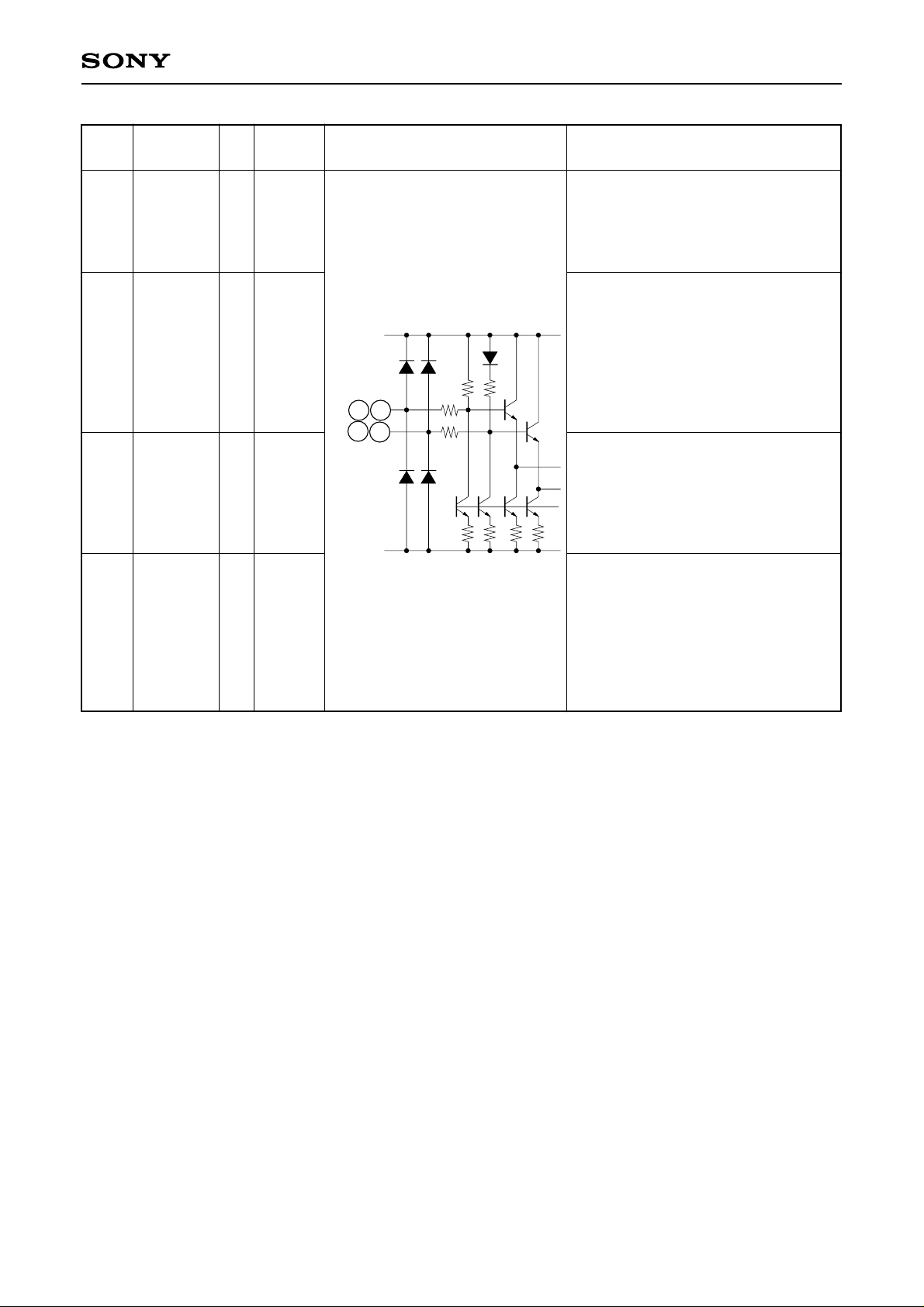
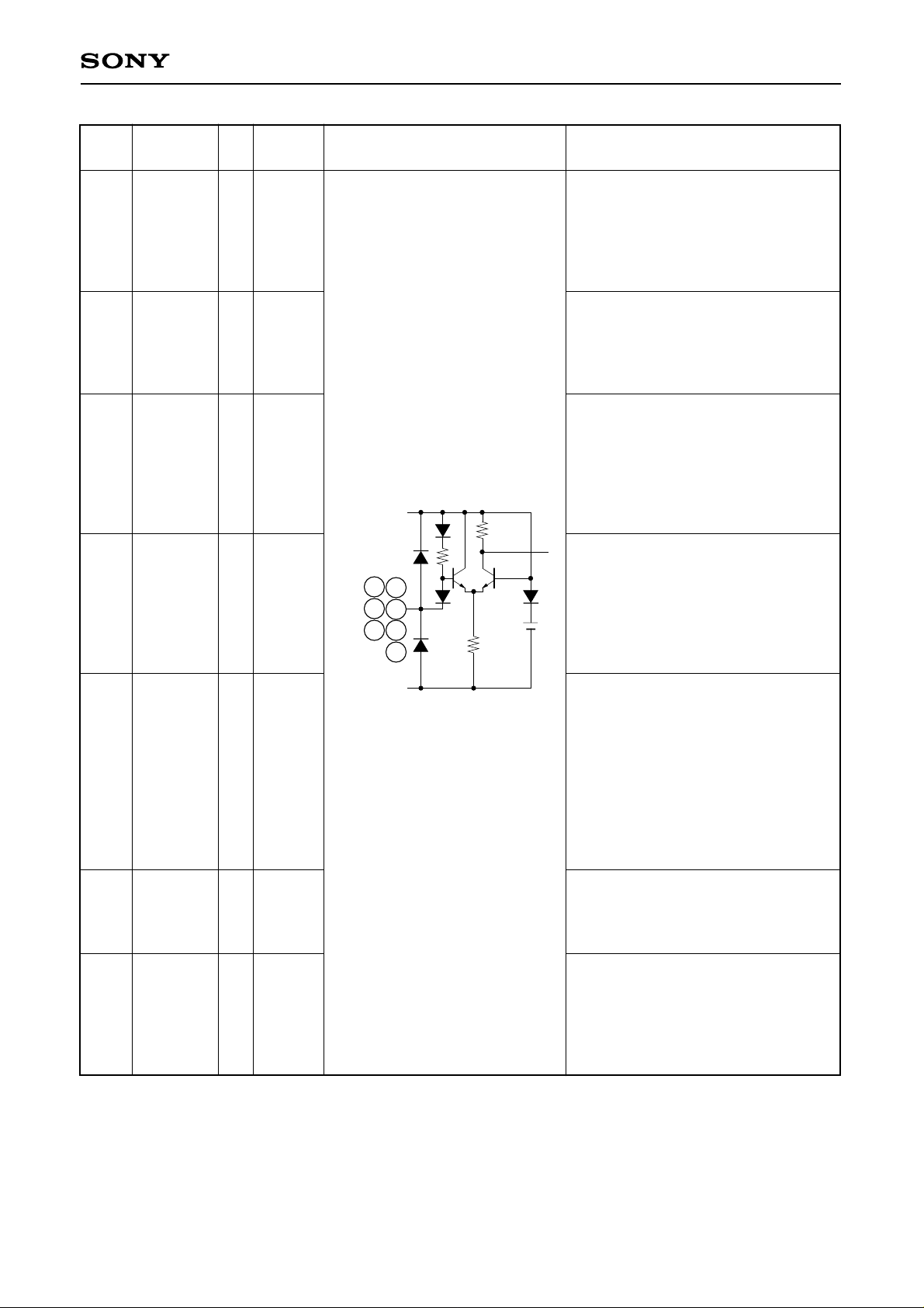
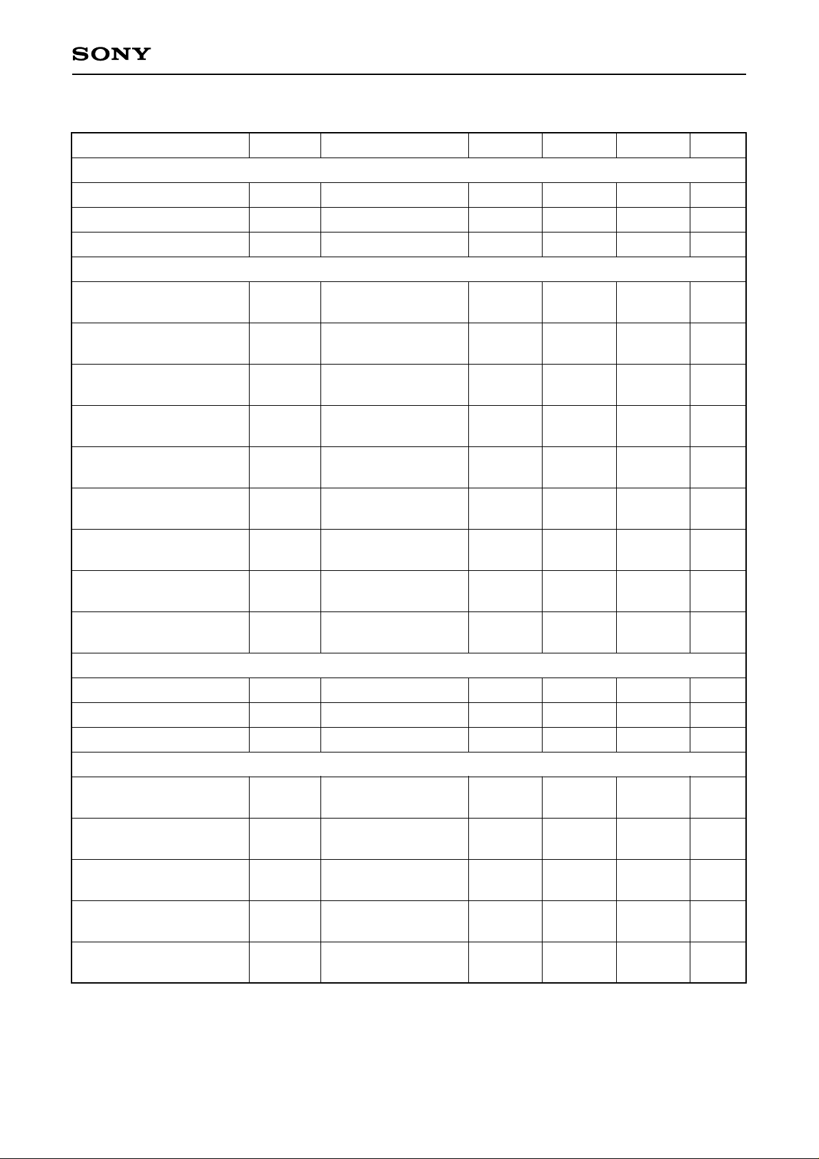
Pin Description and I/O Pin Equivalent Circuit
CXA3106Q
Pin
No.
18
19
25
26
27
28
36
1
2
Symbol I/O
IOVCC
IOGND
DVCC
DGND
TTLGND
TTLVCC
IOGND
PECLVCC
PECLVCC
Reference
voltage level
—
—
—
—
—
—
—
—
—
5V
0V
5V
0V
0V
5V
0V
5V
5V
Equivalent circuit Description
Digital power supply.
Ground this pin to the ground pattern
with a 0.1µF ceramic chip capacitor as
close to the pin as possible.
Digital GND.
Digital power supply.
Digital GND.
TTL output GND.
TTL output power supply.
Ground this pin to the ground pattern
with a 0.1µF ceramic chip capacitor as
close to the pin as possible.
Digital GND.
PECL output power supply.
Ground this pin to the ground pattern
with a 0.1µF ceramic chip capacitor as
close to the pin as possible.
PECL output power supply.
Ground this pin to the ground pattern
with a 0.1µF ceramic chip capacitor as
close to the pin as possible.
37
38
39
40
41
42
43
47
48
IOGND
IOVCC
PLLVCC
PLLGND
VCOVCC
VCOGND
VCOHGND
IRGND
IRVCC
—
—
—
—
—
—
—
—
—
0V
5V
5V
0V
5V
0V
0V
0V
5V
Digital GND.
Digital power supply.
Ground this pin to the ground pattern
with a 0.1µF ceramic chip capacitor as
close to the pin as possible.
PLL circuit analog power supply.
Ground this pin to the ground pattern
with a 0.1µF ceramic chip capacitor as
close to the pin as possible.
PLL circuit analog GND.
VCO circuit analog power supply.
Ground this pin to the ground pattern
with a 0.1µF ceramic chip capacitor as
close to the pin as possible.
VCO circuit analog GND.
VCO SUB analog GND.
IREF analog GND.
IREF analog power supply.
Ground this pin to the ground pattern
with a 0.1µF ceramic chip capacitor as
close to the pin as possible.
– 5 –
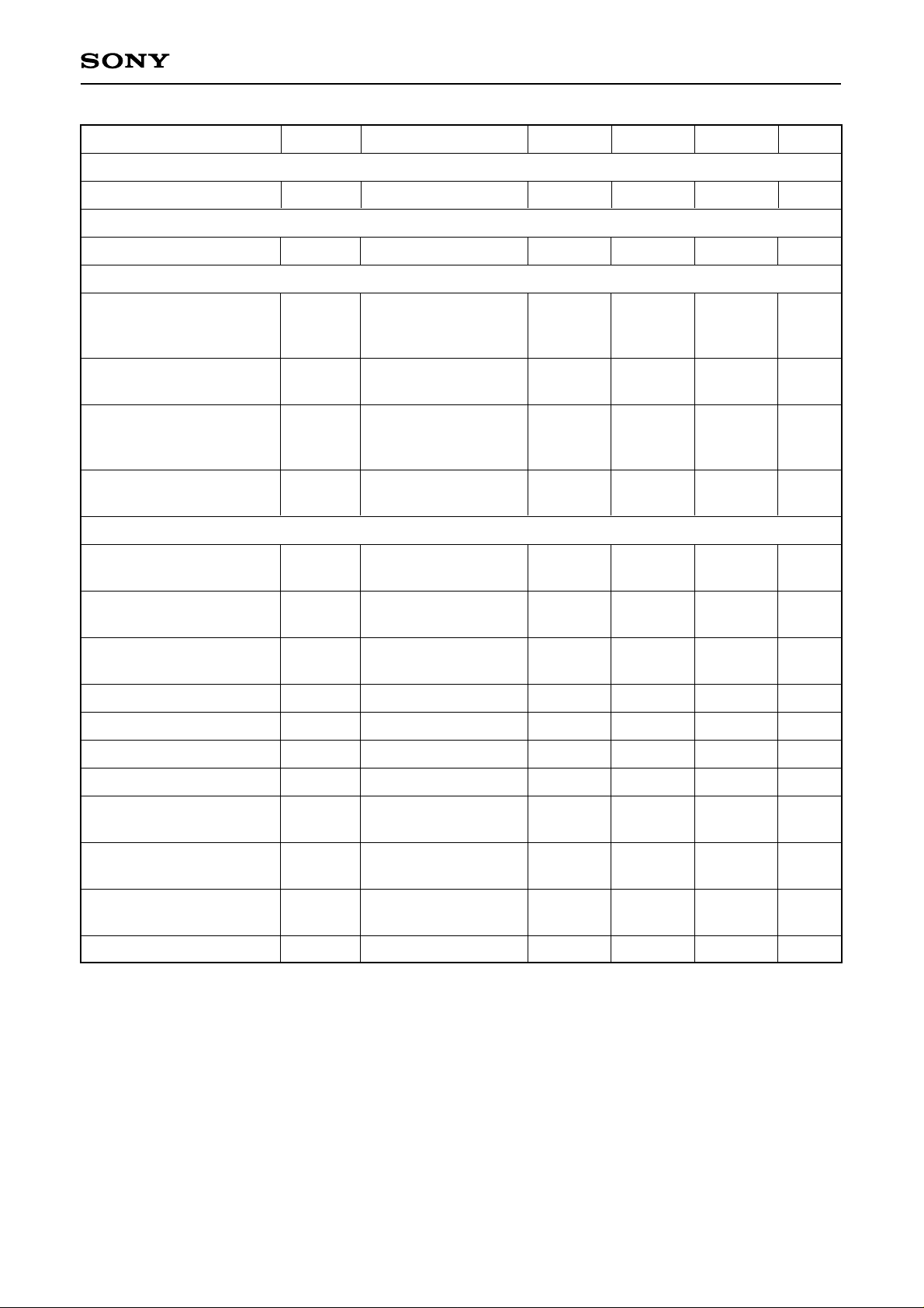
CXA3106Q
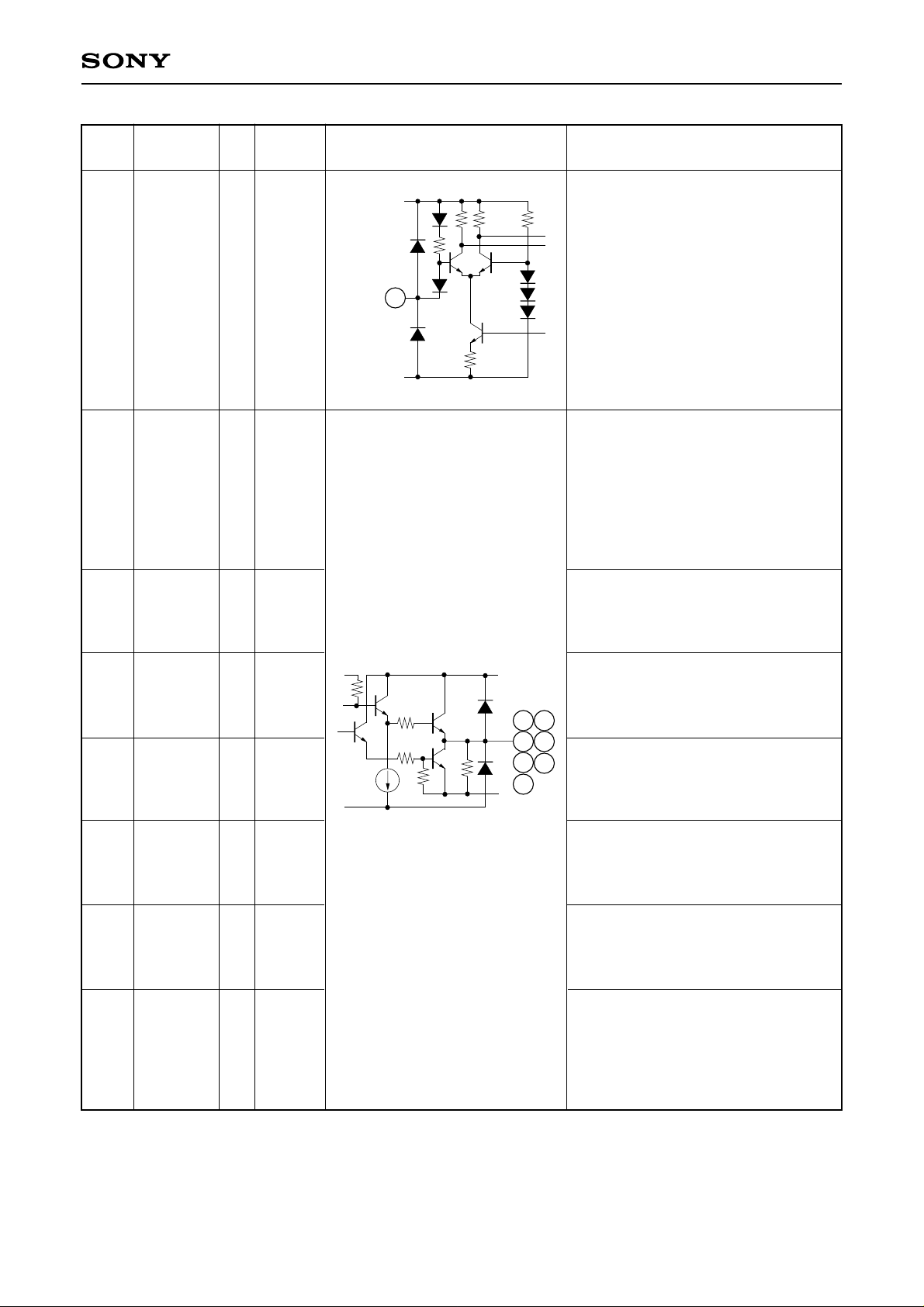
Pin
No.
3
4
7
8
Symbol I/O
VCOH
VCOL
SYNCH
SYNCL
Reference
voltage level
PECL
I
PECL
I
PECL
I
PECL
I
IOV
CC
3
4
IOGND
Equivalent circuit Description
External VCO input.
Programmable counter test input
(switchable by a control register).
When using the VCO PECL input,
open the Pin 5 VCO TTL input.
External inverted VCO input.
When open, this pin goes to the PECL
threshold voltage (IOVcc – 1.3V).
Only the pin 3 VCOH input with VCOL
input open can be also operated but
rr
7
8
complementary input is recommended
in order to realize stable high-speed
operation.
Sync input.
When using the SYNCH PECL input,
open the Pin 9 SYNC TTL input.
The sync signal can be switched
between positive/negative polarity by
an internal register.
Inverted sync input.
When open, this pin goes to the PECL
threshold voltage (IOVcc – 1.3V).
Only the Pin 7 SYNCH input with
SYNCL input open can be also
operated but complementary
input is recommended in order to
realize stable high-speed operation.
– 6 –
CXA3106Q
Pin
No.
10
5
6
9
Symbol I/O
VCO
HOLD
SYNC
SENABLE
Reference
voltage level
TTL
I
TTL
I
TTL
I
TTL
I
Equivalent circuit Description
External VCO input.
Programmable counter test input
(controlled by a control register).
When using the VCO TTL input, open
the Pin 3 VCOH and Pin 4 VCOL
PECL inputs.
Phase detector disable signal.
Active high. When this pin is high, the
phase detector output is held. This pin
goes to high level when open.
(See the HOLD Timing Chart.)
Sync input.
When using the SYNC TTL input,
open the Pin 7 SYNCH and Pin 8
SYNCL PECL inputs.
The sync signal can be switched
IOVCC
5
6
9
10
11
12
13
r/2
r
1.5V
2r
between positive/negative polarity by
a control register.
Control signal (enable) for setting the
internal registers.
When SENABLE is low, registers can
be written; when high, registers can be
read.
(See the Control Register Table and
Control Timing Chart.)
11
12
13
SCLK
SDATA
TLOAD
IOGND
Control signal (clock) for setting the
internal registers.
When SENABLE is low, SDATA is
loaded to the registers at the rising
TTL
I
edge of SCLK.
When SENABLE is high, the register
contents are output from SEROUT at
the falling edge of SCLK.
(See the Control Register Table and
Control Timing Chart.)
Control signal (data) for setting the
TTL
I
internal registers.
(See the Control Register Table and
Control Timing Chart.)
Programmable counter test input.
This pin is normally open status and
TTL
I
high. Register contents can be loaded
immediately to Programmable counter
by setting TLOAD low during the
programmable counter test mode.
– 7 –
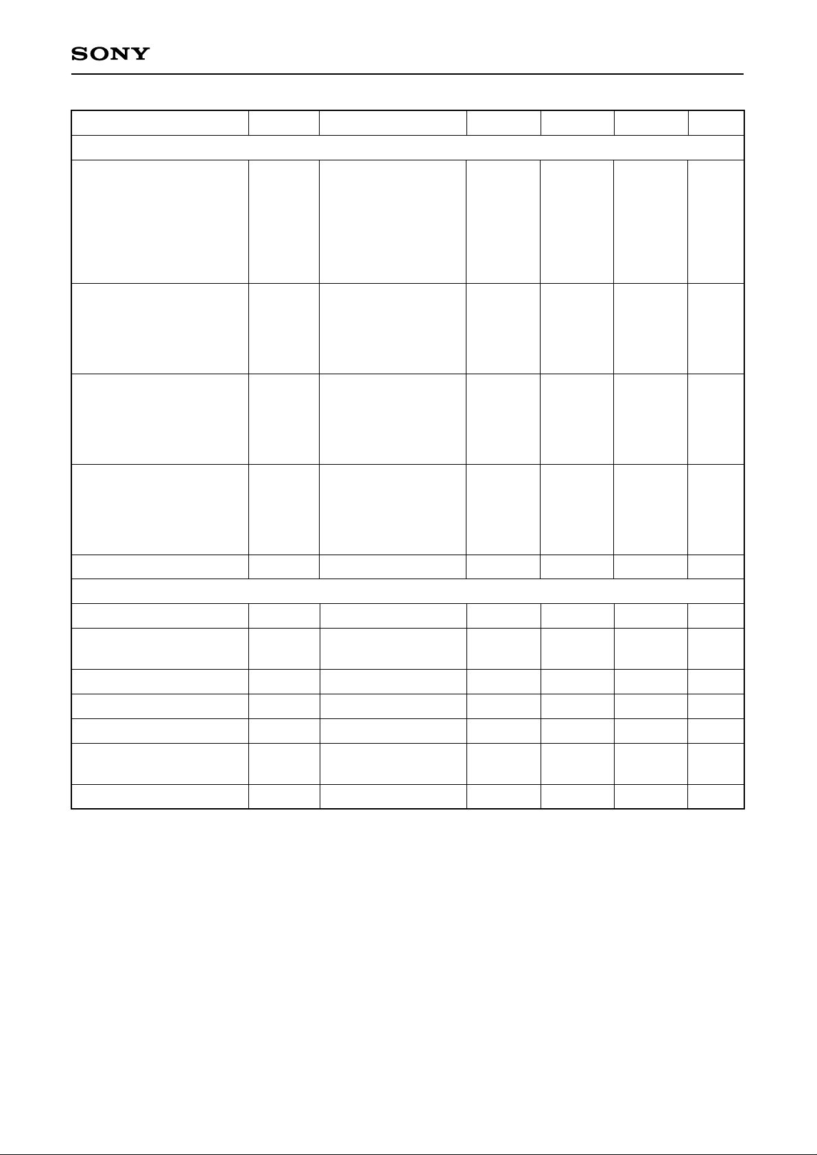
CXA3106Q
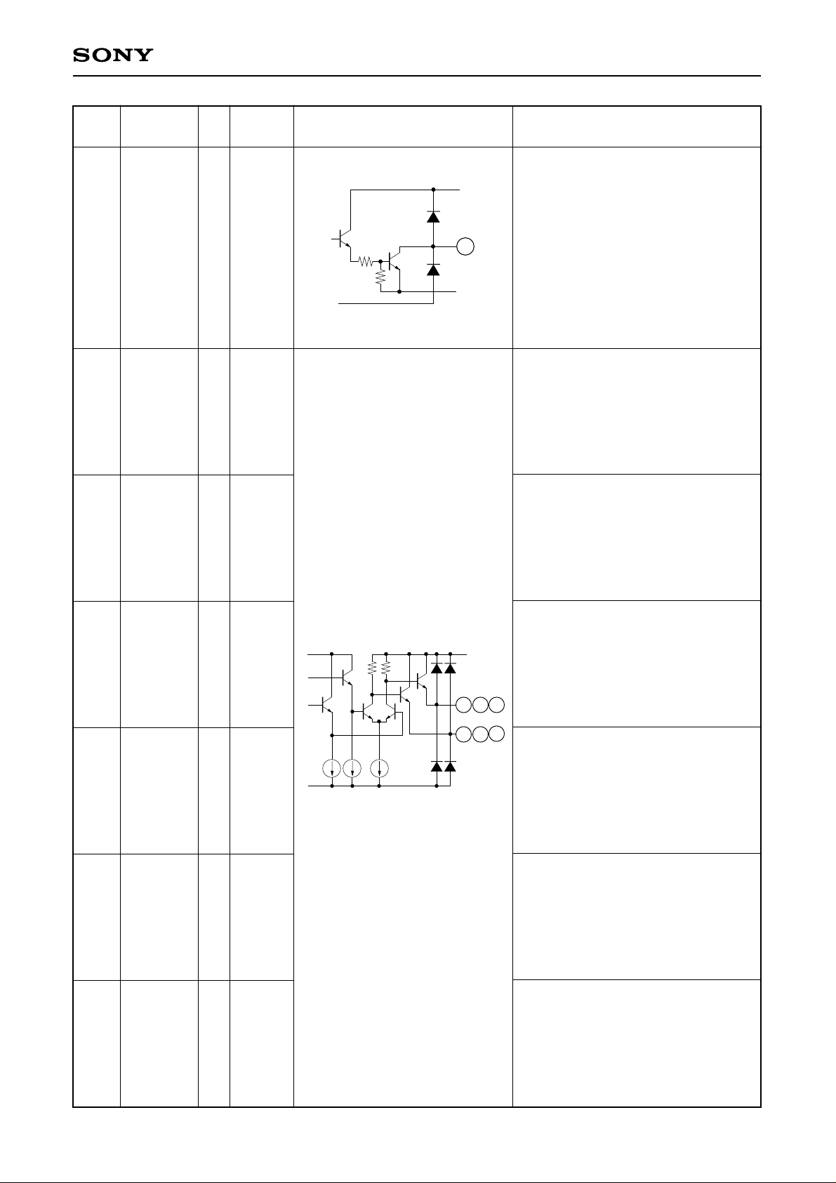
Pin
No.
14
15
16
20
21
22
Symbol I/O
CS
SEROUT
DIVOUT
CLK/2N
CLK/2
CLKN
Reference
voltage level
TTL
I
TTL
O
TTL
O
TTL
O
TTL
O
TTL
O
Equivalent circuit Description
IOVCC
Chip select.
When low, all circuits including the
register circuit are set to the power
14
save mode.
When high, all circuits are set to
operating mode.
IOGND
Register read output.
When SENABLE is high, the register
contents are output from SEROUT at
the falling edge of SCLK.
(See the Control Register Timing
Chart.)
TTL output can be turned ON/OFF
(high impedance) by a control register.
Programmable counter test output.
(See the I/O Timing Chart.)
TTL output can be turned ON/OFF
(high impedance) by a control register.
IOVCC
TTLV
CC
Inverted 1/2 clock output.
(See the I/O Timing Chart.)
TTL output can be turned ON/OFF
15
22
(high impedance) by a control register.
23
1/2 clock output.
24
(See the I/O Timing Chart.)
TTL output can be turned ON/OFF
(high impedance) by a control register.
IOGND
100k
16
20
21
TTLGND
Inverted clock output.
(See the I/O Timing Chart.)
TTL output can be turned ON/OFF
(high impedance) by a control register.
23
24
CLK
DSYNC
Clock output.
TTL
O
(See the I/O Timing Chart.)
TTL output can be turned ON/OFF
(high impedance) by a control register.
Delay sync signal output.
(See the I/O Timing Chart.)
TTL
O
TTL output can be turned ON/OFF
(high impedance) and switched
between positive/negative polarity by
a control register.
– 8 –
CXA3106Q
Pin
No.
17
29
30
Symbol I/O
UNLOCK
CLK/2L
CLK/2H
Reference
voltage level
TTL
O
PECL
O
PECL
O
IOGND
Equivalent circuit Description
Unlock signal output.
TTLVCC
This pin is an open collector output,
and pulls in the current when a phase
difference occurs. The UNLOCK
17
sensitivity can be adjusted by
connecting a capacitor and resistors
to this output as appropriate.
TTLGND
(See the UNLOCK Timing Chart.)
TTL output can be turned ON/OFF
(high impedance) by a control register.
Inverted 1/2 clock output.
(See the I/O Timing Chart.)
This pin requires an external pulldown resistor.
When not used, connect to PECLVCC
without connecting a pull-down
resistor.
1/2 clock output.
(See the I/O Timing Chart.)
This pin requires an external pulldown resistor.
When not used, connect to PECLVCC
without connecting a pull-down
resistor.
31
32
33
34
CLKL
CLKH
DSYNCL
DSYNCH
Inverted clock output.
(See the I/O Timing Chart.)
IOVCC
PECL
O
PECLV
CC
This pin requires an external pulldown resistor.
When not used, connect to PECLVCC
32
30
31
29
without connecting a pull-down
34
resistor.
33
Clock output.
(See the I/O Timing Chart.)
This pin requires an external pull-
PECL
O
IOGND
down resistor.
When not used, connect to PECLVCC
without connecting a pull-down
resistor.
Delay sync signal output.
(See the I/O Timing Chart.)
This pin requires an external pull-
PECL
O
down resistor.
When not used, connect to PECLVCC
without connecting a pull-down
resistor.
Inverted delay sync signal output.
(See the I/O Timing Chart.)
This pin requires an external pull-
PECL
O
down resistor.
When not used, connect to PECLVCC
without connecting a pull-down
resistor.
– 9 –
CXA3106Q
Pin
No.
35
44
Symbol I/O
VBB
IREF
Reference
voltage level
PECLVCC
O
–1.3V
O
1.3V
IOGND
IRVCC
IRGND
IOGND
Equivalent circuit Description
PECLVCC
PECL reference voltage.
When used, ground this pin to the
35
ground pattern with a 0.1µF ceramic
chip capacitor as close to the pin as
possible.
Charge pump current preparation.
Connect to GND via an external
resistor (1.6kΩ).
Ground this pin to the ground pattern
44
with a 0.1µF ceramic chip capacitor
as close to the pin as possible.
45
46
RC2
RC1
External pin for LPF.
See the Recommended Operating
IRV
2.0V
O
to
CC
4.4V
IRGND
O
2.1V
100
VCOVCC
46
45
VCOGND
IOGND
Circuit for the external circuits. Note
that external resistors and capacitors
should be metal film resistors and
temperature compensation capacitors
which are relatively unaffected by
temperature change.
External pin for LPF.
See the Recommended Operating
Circuit for the external circuits.
– 10 –
CXA3106Q
LSB
ADDR0
ADDR1
MSB
ADDR2
DATA0
DATA1
DATA2
1
0
0
8
7
6
DIV
VCO
DIV
VCO
DIV
VCO
Bit 0
Bit 1
Bit 2
12
11
10
0
1
0
DIV
VCO
DIV
VCO
DIV
VCO
Bit 8
Bit 9
Bit 10
19
18
17
1
1
0
26
25
24
0
0
1
FINE
DELAY
FINE
DELAY
FINE
DELAY
Bit 0
Bit 1
Bit 2
29
28
27
1
0
1
Bit 0
C.Pump
Bit 1
C.Pump
PD
POL
37
36
35
0
1
1
POL
SYNC
POL
DSYNC
CLK
Enable
41
40
39
1
1
1
VCO
By-pass
Synth
power
power
Read out
DATA3
DATA ADDRESS
DATA4
DATA5
DAT6
MSB1VCO
DATA7
Register Name
5
VCO
4
VCO
3
VCO
2
VCO
DIV
DIV
DIV
DIV
DIV
Bit 3
Bit 4
Bit 5
Bit 6
Bit 7
9
DIVREG1
register read no
register read no
DIV
VCO
Bit 11
DIVREG2
16
15
14
Bit 0
23
22
21
DIV 1, 2, 4
13
Bit 1
20
DIV 1, 2, 4
CENFREREG
register read no
register read no
Bit 3
FINE
DELAY
Bit 4
FINE
DELAY
Bit 0
DELAY
COARSE
Bit 1
DELAY
COARSE
DELAYREG
34
33
32
31
30
CPREG
register read no
register read no
38
NCLK
Enable
CLK/2
Enable
Enable
NCLK/2
Enable
DSYNC
Enable
UNLOCK
TTLPOLREG
register read no
Enable
DIVOUT
TESTPOWREG
Register No.
Register 1
Control Register Table
Register 2
Register 3
– 11 –
Register 4
Register 5
Register 6
Register 7
CXA3106Q
Electrical Characteristics (Ta = 25°C, VCC = 5V, GND = 0V)
Item Symbol Conditions Min. Typ. Max. Unit
Current consumption (excluding output current)
Current consumption 1
Current consumption 2
Current consumption 3
Digital input
Digital high level input
voltage (PECL)
Digital low level input
voltage (PECL)
VCOL, SYNCL input open
voltage (PECL)
Digital high level input
current (PECL)
Digital low level input
current (PECL)
Digital high level input
voltage (TTL)
Digital low level input
voltage (TTL)
Digital high level input
current (TTL)
ICC1
ICC2
ICC3
VIH1
VIL1
VIO
IIH1
IIL1
VIH2
VIL2
IIH2
CS = H, Synth Power = 1
CS = H, Synth Power = 0
CS = L
VIH = IOVCC – 0.8V
VIL = IOVCC – 1.6V
VIH = 2.7V
40
5
3
IOVCC
–1.15
–100
–200
2.0
–200
67
15
10
IOVCC
–1.3
100
30
20
IOVCC
–1.5
100
0
0.8
–20
mA
mA
mA
V
V
V
µA
µA
V
V
µA
Digital low level input
current (TTL)
HOLD characteristics
RC1 input pin leak current
HOLD signal set-up time
HOLD signal hold time
Digital output
Digital high level output
voltage (PECL)
Digital low level output
voltage (PECL)
PECL output reference
voltage
Digital high level output
voltage (TTL)
Digital low level output
voltage (TTL)
IIL2
Ileak
Ths
Thh
VOH1
VOL1
VBB
VOH2
VOL2
VIL = 0.5V
RL = 330Ω
RL = 330Ω
RL = 330Ω
CL = 10pF
CL = 10pF
–500
20
20
PECLVCC
–1.1
2.7
PECLVCC
–1.3
–100
1.00
PECLVCC
–1.6
0.5
µA
nA
ns
ns
V
V
V
V
– 12 –
Item Symbol Conditions Min. Typ. Max. Unit
UNLOCK output
CXA3106Q
UNLOCK output current
SYNC input
SYNC input frequency range
DSYNC output
DSYNC output variable
coarse delay time setting
resolution
DSYNC output variable
coarse delay time
DSYNC output variable
fine delay time setting
resolution
DSYNC output variable
fine delay time
VCO characteristics
DIV output frequency
operation range 1
DIV output frequency
operation range 2
Iunlock
Fin
Rdsync1
Td1
Rdsync2
Td2
FVCO1
FVCO2
DIV = 1/1
DIV = 1/2
–30
10
1
1/16
40
20
mA
100
2
4
5
20/16
120
60
kHz
bit
CLK
bit
CLK
MHz
MHz
DIV output frequency
operation range 3
VCO lock range
VCO gain 1
VCO gain 2
VCO gain 3
Charge pump current 1
Charge pump current 2
Charge pump current 3
VCO counter bits
FVCO3
Vlock
KVCO1
KVCO2
KVCO3
Kpd1
Kpd2
Kpd3
Rdiv2
DIV = 1/4
DIV = 1/1
DIV = 1/2
DIV = 1/4
C.Pump Bit = 00,
IREF = 1.6kΩ
C.Pump Bit = 10,
IREF = 1.6kΩ
C.Pump Bit = 11,
IREF = 1.6kΩ
10
2.0
200
100
50
80
350
1350
320
160
80
100
400
1600
12
30
4.4
550
270
135
130
500
1800
MHz
V
Mrad/sv
Mrad/sv
Mrad/sv
µA
µA
µA
bit
– 13 –

Item Symbol Conditions Min. Typ. Max. Unit
CLK (CLK, CLK/2) output
CXA3106Q
CLK output (PECL)
frequency range 1
CLK output (PECL)
frequency range 2
CLK output (PECL)
frequency range 3
CLK, CLK/2 output (PECL)
rise time
CLK, CLK/2 output (PECL)
fall time
CLK output (TTL)
frequency range 1
CLK output (TTL)
frequency range 2
CLK output (TTL)
frequency range 3
CLK, CLK/2 output (TTL)
rise time
CLK, CLK/2 output (TTL)
fall time
Fclk1PECL
Fclk2PECL
Fclk3PECL
TrPECL
TfPECL
Fclk1TTL
Fclk2TTL
Fclk3TTL
TrTTL
TfTTL
DIV = 1/1
DIV = 1/2
DIV = 1/4
10% to 90%,
RL = 330Ω
10% to 90%,
RL = 330Ω
DIV = 1/1
DIV = 1/2
DIV = 1/4
10% to 90%,
CL = 10pF
10% to 90%,
CL = 10pF
40
20
10
1.0
1.0
40
20
10
2.0
2.0
1.5
1.5
3.0
3.0
120
60
30
2.0
2.0
80
60
30
4.0
4.0
MHz
MHz
MHz
ns
ns
MHz
MHz
MHz
ns
ns
CLK output (PECL, TTL)
duty
SYNC input (PECL) and
CLK output (PECL) delay
offset
CLK output (PECL) and
DSYNC output (PECL)
phase difference
CLK output (PECL) and
CLK/2 output (PECL)
phase difference
CLK output (PECL) and
DIVOUT output (TTL) rise
phase difference
CLK output (PECL) and
DIVOUT output (TTL) fall
phase difference
DSYNC, CLK, CLK/2 PECL
output and TTL output
phase difference
Dclk2
Td3
Td4
Td5
Td6
Td7
Td8
CL = 10pF
CL = 10pF
CL = 10pF
CL = 10pF
CL = 10pF
CL = 10pF
CL = 10pF
40
1.5
0.0
1.5
50
1
2.4
0.8
14
11
3.0
60
3.0
1.0
4.5
%
ns
ns
ns
ns
ns
ns
– 14 –
Item Symbol Conditions Min. Typ. Max. Unit
CLK (CLK, CLK/2) output
CLK vs. SYNC output jitter
(NTSC)
CLK vs. SYNC output jitter
(VGA)
CLK vs. SYNC output jitter
(SVGA)
Tj1p-p
Tj2p-p
Tj3p-p
triggered at SYNC
Fsync = 15.73kHz
(Crystal)
Fclk = 12.27MHz
N = 780
Fine Delay =
2/16 to 20/16
triggered at SYNC
Fsync = 31.47kHz
(Crystal)
Fclk = 25.18MHz
N = 800
triggered at SYNC
Fsync = 48.08kHz
(Crystal)
Fclk = 50.00MHz
N = 1040
4.0
3.0
2.0
7.0
5.0
3.0
CXA3106Q
ns
ns
ns
CLK vs. SYNC output jitter
(XGA)
CLK vs. DSYNC output jitter
Control registers
SCLK frequency
SENABLE setup time
SENABLE hold time
SDATA setup time
SDATA hold time
SENABLE setup time
SENABLE hold time
Tj4p-p
Tj5p-p
SCLK
TENS
TENH
TDS
TDH
TNENS
TNENH
triggered at SYNC
Fsync = 56.48kHz
(Crystal)
Fclk = 75.00MHz
N = 1328
triggered at DSYNC
in write/read mode
in write mode
in write mode
in write mode
in read mode
in read mode
in read mode
1.6
3
0
3
0
3
0
2.5
0.1
12
ns
ns
MHz
ns
ns
ns
ns
ns
ns
– 15 –
 Loading...