

Sony CXA3099N Datasheet

—1—
E95Y24A8Z
Sony reserves the right to change products and specifications without prior notice. This information does not convey any license by
any implication or otherwise under any patents or other right. Application circuits shown, if any, are typical examples illustrating the
operation of the devices. Sony cannot assume responsibility for any problems arising out of the use of these circuits.
Absolute Maximum Ratings
• Supply voltage VCC 7.0 V
• Operating temperature Topr –20 to +75 °C
• Storage temperature Tstg –65 to +150 °C
• Allowable power dissipation PD 312 mW
Operating Condition
Supply voltage VCC1 1.1 to 4.0 V
Description
The CXA3099N is a low current consumption FM
IF amplifier which employs the newest bipolar
process. It is suitable for M-ary FSK pagers.
Features
• Low current consumption: 590 µA
(typ. at VCC = 1.4 V)
• Low voltage operation: VCC = 1.1 to 4.0 V
• Small package 16-pin SSOP
• Needless of IF decoupling capacitor
• Reference power supply for operational amplifier
and comparator
• IF input, VCC standard
Applications
M-ary FSK pagers
Structure
Bipolar silicon monolithic IC
IF Amplifier for M-ary FSK Pagers
16 pin SSOP (Plastic)
CXA3099N
For the availability of this product, please contact the sales office.
—2—
CXA3099N
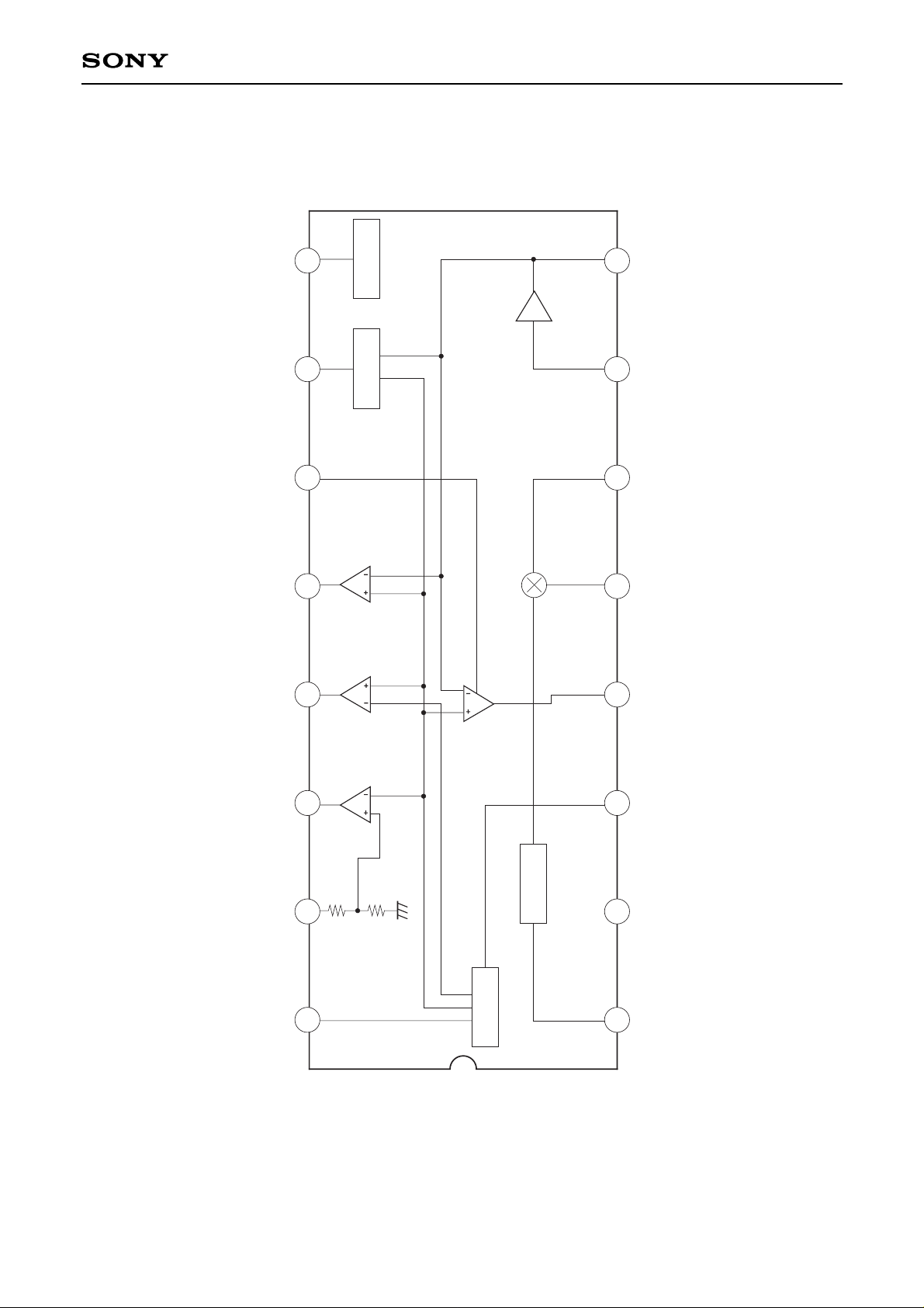
RSSIDEV COMP
VCC REG OUT REG CONT LVA OUT NRZ OUT CHARGE DEV OUT RSSI
LPF OUTLPF INDET OUTQUADFSK REFBSGNDIF IN
78k
R2
22k
R1
GND
REG
IF LIM
101112131416
9
15
2 3 4 5 6 71 8
CHARGE
QUAD DET
VB REG NRZ COMP
LVA
Block Diagram and Pin Configuration
—3—
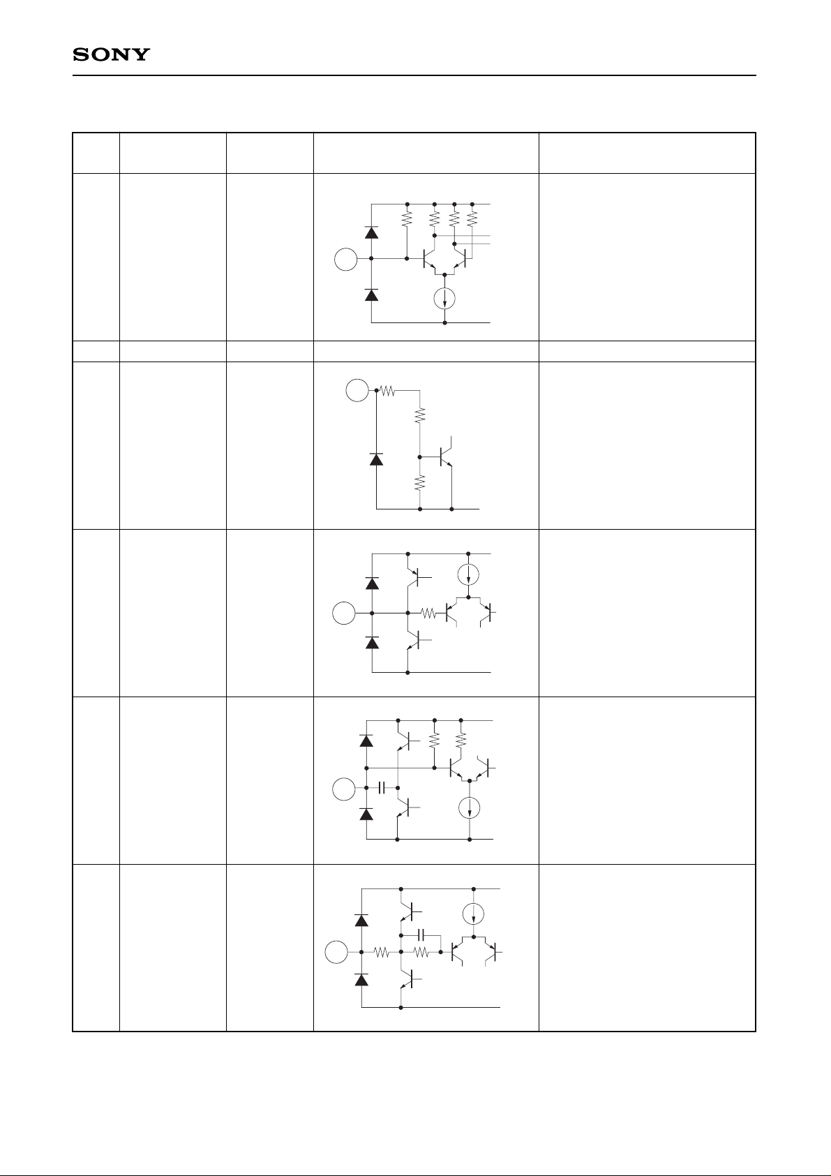
CXA3099N
Pin Description
Pin
No.
Symbol Pin voltage Equivalent circuit Description
1
2
3
4
5
6
IF IN
GND
B.S.
FSK REF
QUAD
DET OUT
1.4 V
—
—
0.2 V
1.4 V
0.2V
IF limiter amplifier input.
Ground.
Controls the battery saving.
Setting this pin low suspends the
operation of IC. (Applied voltage
range: –0.5 V to +7.0 V)
Connects the capacitor that
determines the low cut-off
frequency for the entire system.
Connects the phase shifter of FM
detector circuit.
FM detector output.
VCC
1.5k
GND
1.5k
20k 20k
1
72
40k
140k
GND
3
VCC
GND
72
4
VCC
22k
GND
20p
20k
5
VCC
GND
50p
55k
72
6
—4—
CXA3099N
Pin
No.
Symbol Pin voltage Equivalent circuit Description
7
8
9
10
12
13
11
LPF IN
LPF OUT
RSSI
DEV OUT
NRZ OUT
LVA OUT
CHARGE
0.2 V
0.2 V
0 V
—
—
—
0 V
Operational amplifier input.
Level comparator and NRZ
comparator inputs. Output for
operational amplifier is
connected.
RSSI circuit output.
Level comparator, NRZ
comparator and LVA comparator
outputs. They are open
collectors. (Applied voltage
range: –0.5 V to +7.0 V)
Controls the ON/OFF operation
of the quick-charge circuit.
Set this pin high to execute the
quick charge. (Applied voltage
range: –0.5 V to +7.0 V)
VCC
GND
72
7
VCC
GND
72
72
8
VCC
GND
7k 7k
70k
9
72
GND
10
12
13
20k
100k
GND
11
—5—
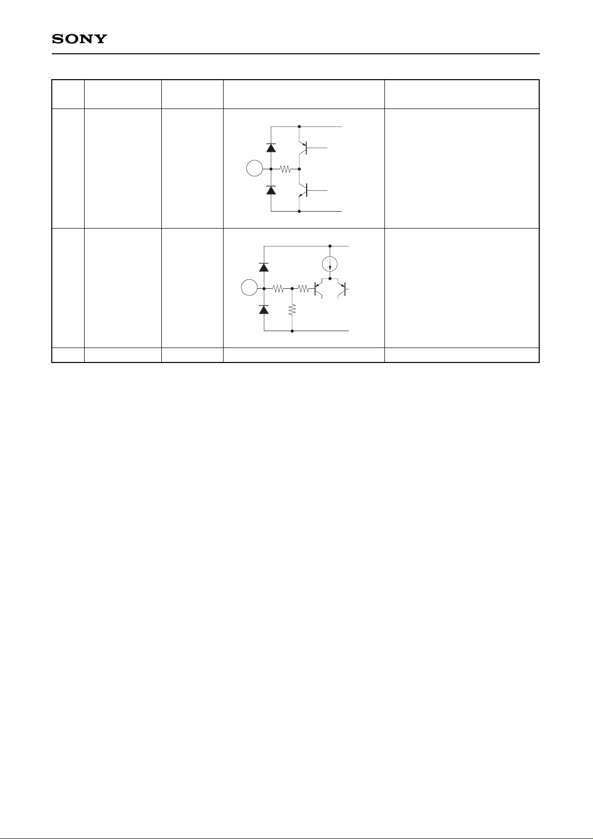
CXA3099N
Pin
No.
Symbol Pin voltage Equivalent circuit Description
14
15
16
REG CONT
REG OUT
VCC
—
1.0 V
Output for internal constantvoltage source amplifier.
Connect the base of PNP
transistor.
(Current capacity: 100 µA)
Constant-voltage source output.
Controlled to maintain 1.0 V.
Power supply.
VCC
GND
72
14
VCC
GND
78k
1k
22k
15
 Loading...