

Sony CXA3071N Datasheet

– 1 –
CXA3071N
E96146B8Z
Read/Write Amplifier (with Built-in Filters) for FDDs
Description
The CXA3071N is a monolithic IC designed for use
with three-mode Floppy Disk Drives, and contains a
read circuit (with a four-mode filter system), a write
circuit, an erase circuit, and a supply voltage
detection circuit, all on a single chip.
Features
• Single 5V power supply
• All filter, write current and other characteristics can
be set with a single external resistor.
• Filter system can be switched among four modes:
1M, 1.6M/2M, which are each inner track/outer
track.
• Filter characteristics can be set to Chebyshev (1dB
ripple) for 1.6M, 2M/inner track only, and to
Butterworth for the other modes and a custom
selection can be made between Chebyshev (1dB
ripple) and Butterworth for 1.6M, 2M/inner track
only.
• 1M/outer track f0 and the fc ratio for each mode
can be customized.
• Preamplifier voltage gain can be set to 45dB or
48dB by switching the filter mode and inner/outer
track.
• Preamplifier and filter output are monitored with
the same pins. These pins are normally set to filter
output, but the preamplifier output can be
monitored by temporarily setting the SETR pin (Pin
20) to Low.
• Time domain filter can be switched between two
modes: 1M, 1.6M/2M.
In addition, the pulse width can be customized.
• Write current can be switched among six modes
according to the mode and inner/outer track
setting.
The current value can be customized for each
mode.
• Erase current remains constant, and the current
value can be customized.
• Damping resistor can be built in. Resistor can be
customized between 2kΩ and 15kΩ in 1kΩ steps.
• Supply voltage detection circuit
Applications
Three-mode FDDs
Structure
Bipolar silicon monolithic IC
Absolute Maximum Ratings (Ta = 25°C)
• Supply voltage VCC 7.0 V
• Digital signal input pin voltage
–0.5 to VCC + 0.3 V
• Power ON output applied voltage
VCC + 0.3 V
• Erase output applied voltage VCC + 0.3 V
• Write head applied voltage 15 V
• Power ON output current 7 mA
• Operating temperature Topr –20 to +75 °C
• Storage temperature Tstg –65 to +150 °C
• Allowable power dissipation
PD 375 mW
Operating Conditions
Supply voltage 4.4 to 6.0 V
Sony reserves the right to change products and specifications without prior notice. This information does not convey any license by
any implication or otherwise under any patents or other right. Application circuits shown, if any, are typical examples illustrating the
operation of the devices. Sony cannot assume responsibility for any problems arising out of the use of these circuits.
20 pin SSOP (Plastic)
For the availability of this product, please contact the sales office.
– 2 –
CXA3071N
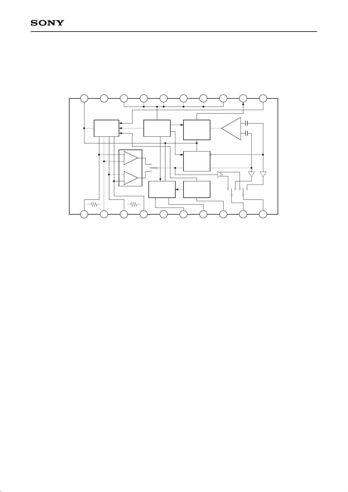
Block Diagram and Pin Configuration
WRITE
DRIVER
COMP
PREAMP
CONTROL
LOGIC
TIME
DOMAIN
FILTER
FILTER
DIFF + LPF
(BPF)
POWER
MONITOR
ERASE
DRIVER
2
3
4
5
6
7
8
9
10
1
11
12
13
14
15
16
17
18
19
20
HEAD1A
HEAD1B
HEAD0A
HEAD0B
GND
ERA0
ERA1
PONOUT
MONITORA
MONITORB
SETR
V
CC
X360
XHD
OTF
XS1
XEG
WG
RD
XWD
– 3 –
CXA3071N
Pin Description
Pin
No.
Symbol
Pin
voltage
Equivalent circuit Description
1
2
3
4
HEAD1A
HEAD1B
HEAD0A
HEAD0B
—
—
—
—
Magnetic head inputs/outputs.
Connect the recording/playback magnetic
head to these pins, and connect the center
tap to V
CC. When the logical voltage for
Pin 15 (XS1) is Low, the HEAD1 system is
active; when the logical voltage is High,
the HEAD0 system is active.
GND
2
3
4
1
5
GND —
GND connection.
6 ERA0
—
7
ERA1
—
8
9
10
PON
OUT
—
MONITORA
4.0V
during
filter
output
3.4V
during
preamplifier
output
4.0V
during
filter
output
3.4V
during
preamplifier
output
MONITORB
Erase output for the HEAD0 system.
Erase output for the HEAD1 system.
Reduced voltage detection output. This is
an open collector that outputs a low signal
when VCC is below the specified value.
MONITOR differential outputs.
These pins are set to filter output during
normal read mode, but the preamplifier
output can be monitored by temporarily
setting Pin 20 (SETR) to Low.
VCC
GND
6
7
VCC
GND
8
100k 100k
500µ500µ
9
10
V
CC
GND
– 4 –
CXA3071N
11 XWD —
Write data input. This pin is a Schmitttype input that is triggered when the
logical voltage goes from High to Low.
VCC
1k
GND
2.3V
11
140
V
CC
GND
12
GND
0.65
V
CC
0.35
VCC
13
147
VCC
0.5
VCC
VCC
100k
1k
GND
2.1V
14
15
16
17
18
12
13RDWG
—
0.5VCC
during
read
Read data output.
This pin is active when the logical voltage
of the write gate signal and the erase gate
signal is High.
WG signal input.
The write system becomes active when
the logical voltage is High.
The IC is in power saving mode when the
logical voltage is Low.
The read system becomes active when
the logical voltage is Z.
14
XEG
—
XEG signal input. The erase system
becomes active when the logical voltage
is Low.
15
XS1
—
16
OTF
—
—
—
Head side switching signal input. The
HEAD1 system is active when the logical
voltage is Low, and the HEAD0 system is
active when the logical voltage is High, but
only when the logical voltage for the WG
signal is Z and of the XEG signal is High.
Filter inner track/outer track mode control.
Outer track mode is selected when the
logical voltage is High.
Filter, time domain filter and write current
1M/2M mode control. 1.6M/2M mode is
selected when the logical voltage is Low.
17
18
19
XHD
X360
VCC
—
Filter, time domain filter and write current
1.6M/2M mode control. 1.6M mode is
selected when the logical voltage is Low.
Power supply (5V) connection.
Pin
No.
Symbol
Pin
voltage
Equivalent circuit Description

– 5 –
CXA3071N
3.8V
20 SETR
Filter cutoff frequency, time domain filter
1st monostable multivibrator pulse width,
read data, write current and erase current
setting resistor connection. Connect the
setting resistor R between this pin and
VCC.
Pin
No.
Symbol
Pin
voltage
Equivalent circuit Description
147
VCC
20
1.2V
GND

– 6 –
CXA3071N
Electrical Characteristics
Current Consumption (Ta = 25°C, VCC = 5V)
Current consumption
in read mode
Current consumption
in write/erase mode
Current consumption
in power saving
mode
ICCR
ICCWE
ICCPS
WG = "Z"
WG = "H", XEG = "L"
WG = "L"
—
—
—
—
—
—
15.0
11.0
—
25.0
17.0
1.2
35.0
23.0
2.0
mA
mA
mA
Power Supply Monitoring System (Ta = 25°C)
Power supply
ON/OFF detector
threshold voltage
Power ON output
saturation voltage
VTH
VSP
VCC = 3.5V
I = 1mA
—
—
—
—
3.5—3.9—4.3
0.5VV
Read System (Ta = 25°C, VCC = 5V)
Preamplifier
voltage gain
1M/outer track
Preamplifier
voltage gain
1M/inner track
Preamplifier
voltage gain
1.6M, 2M/
outer track
Preamplifier
voltage gain
1.6M, 2M/
inner track
Preamplifier
frequency
response
Preamplifier
input
conversion
noise voltage
GVLO
GVLI
GVHO
GVHI
BWO
ENO
f = 100kHz, OTF = "H",
XHD = "H", X360 = "X"
f = 100kHz, OTF = "L",
XHD = "H", X360 = "X"
f = 100kHz, OTF = "H",
XHD = "L", X360 = "X"
f = 100kHz, OTF = "L",
XHD = "L", X360 = "X"
GV/GV0 = –3dB
BW = 400Hz to 1MHz,
VI = 0
1
1
1
1
1
1
A, B
A, B
A, B
A, B
A, B
A, B
43.1
46.1
43.1
46.1
5
—
45.0
48.0
45.0
48.0
—
2.0
46.6
49.6
46.6
49.6
—
2.9
dB
dB
dB
dB
MHz
nV/√Hz
Item Symbol
Conditions
Measurement
circuit
Measurement
point
Min. Typ. Max. Unit
Item Symbol
Conditions
Measurement
circuit
Measurement
point
Min. Typ. Max. Unit
Item Symbol
Conditions
Measurement
circuit
Measurement
point
Min. Typ. Max. Unit

– 7 –
CXA3071N
Read System (Ta = 25°C, VCC = 5V)
Filter output voltage
amplitude
Time domain filter
monostable
multivibrator pulse
width
Read data pulse
width
Read data output low
output voltage
Read data output
high output voltage
Read data output
∗1
rise time
Read data output
∗1
fall time
Peak shift
∗2
VOF
T1
T2
VOL
VOH
tr
tf
PS
X360 = "X", XHD = "H"
(1M mode)
X360 = "X", XHD = "L"
(1.6M/2M mode)
IOL = 2mA
IOH = –0.4mA
RL = 2kΩ
CL = 20pF
RL = 2kΩ
CL = 20pF
VI = 0.25mVp-p to
3.5mVp-p
X360 = "H", XHD = "L"
OTF = "L"
f = 125kHz,
2M/inner track mode
1
1
1
1
1
1
1
1
1
A, B
C, D
C, D
D
D
D
D
D
D
1.4
2.25
1.16
300
—
2.8
—
—
—
—
2.50
1.29
400
—
—
—
—
—
—
2.75
1.42
500
0.5
—
100
100
1
Vp-p
µs
µs
ns
V
V
ns
ns
%
∗1
Read data output: 0.5V to 2.4V
∗2
Signal input level
1M, 1.6M, 2M/outer track: VI = 0.25mVp-p to 5mVp-p
1M, 1.6M, 2M/inner track: VI = 0.25mVp-p to 3.5mVp-p
Item Symbol Conditions
Measurement
circuit
Measurement
point
Min. Typ. Max. Unit
– 8 –
CXA3071N
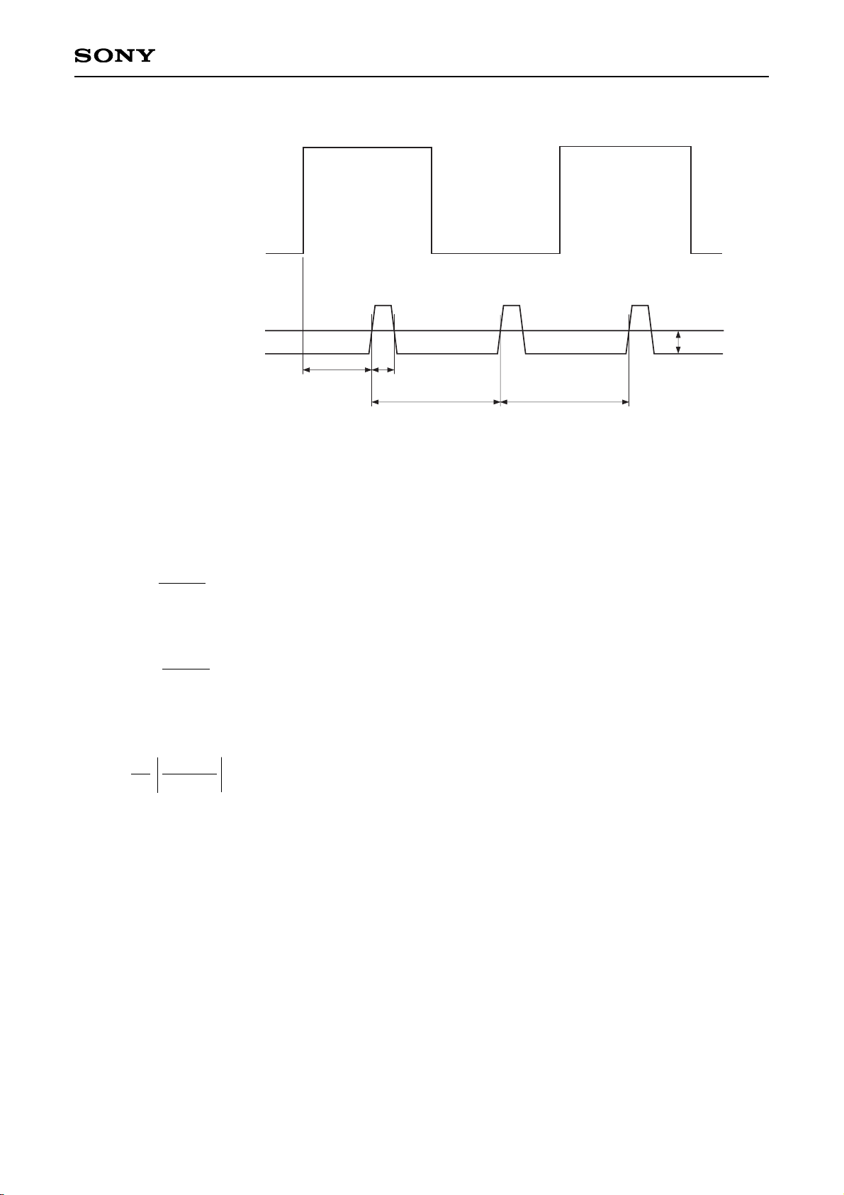
Fig. 1. 1st and 2nd monostable multivibrator pulse width precision
and peak shift measurement conditions
• 1st monostable multivibrator pulse width precision
When X360 = "X" and XHD = "H":
ETM1 = ( –1) × 100 [%]
When X360 = "X" and XHD = "L":
ETM1' = ( –1) × 100 [%]
• 2nd monostable multivibrator pulse width = T2
• Peak shift
PS = × 100 [%]
T1
2.5µs
12TA – TB
TA + TB
T1
1.29µs
External Comparator Output
(Measurement point C)
T1 T2
TA TB
1.4V
Read data output
(Measurement point D)
 Loading...