

Sony CXA3031Q Datasheet

– 1 –
CXA3031Q
E95318-ST
Read/Write Amplifier (with Built-in Filters) for FDDs
Description
The CXA3031Q is a monolithic IC designed for use
with three-mode Floppy Disk Drives, and contains a
read circuit (with a four-mode filter system), a write
circuit, an erase circuit, and a supply voltage
detection circuit, all on a single chip.
Features
• Single 5V power supply
• Filter system can be switched among four modes:
1M, 1.6M/2M, which are each inner track/outer
track
• Filter characteristics can be set to Chebyshev (1dB
ripple) for 1.6M, 2M/inner track only, and to
Butterworth for the other modes
• A custom selection can be made between
Chebyshev (1dB ripple) and Butterworth for the
filter characteristics for 1.6M, 2M/inner track only
• Permits customization of the fc ratio
• Low preamplifier input conversion noise voltage of
2.0nV/√ Hz (typ.) keeps read data output jitter to a
minimum
• Preamplifier voltage gain can be switched between
39dB and 45dB
• In inner track mode (OTF = Low), the voltage gain
is boosted by 3dB, making it possible to minimize
peak shift in inner tracks.
• Time domain filter can be switched between two
modes: 1M, 1.6M/2M
• Write current can be switched among three modes:
1M/1.6M/2M. The inner/outer track current ratio is
fixed for each mode, but can be customized.
• Erase current can be set by an external resistor,
and remains constant. In addition, the current rise
time Tr and fall time Tf are determined according to
the head inductance and current. (Refer to page
20.)
• Damping resistor can be built in. Resistance can be
customized between 2kΩ and 15kΩ in 1kΩ steps.
A damping resistor can not be connected to this IC,
however.
• Supply voltage detection circuit
Applications
Three-mode FDDs
Structure
Bipolar silicon monolithic IC
Absolute Maximum Ratings (Ta = 25°C)
• Supply voltage VCC 7.0 V
• Operating temperature Topr –20 to +75 °C
• Storage temperature Tstg –65 to +150 °C
• Allowable power dissipation
PD 500 mW
• Digital signal input pin Input voltage
–0.5 to VCC + 0.3 V
• Power ON output voltage applied VCC + 0.3 V
• Erase output voltage applied VCC + 0.3 V
• Write head voltage applied 15 V
• Write current IW 20 mAo-p
• Erase current IE 30 mA
• Power on output current 7 mA
Operating Conditions
Supply voltage 4.4 to 6.0 V
Sony reserves the right to change products and specifications without prior notice. This information does not convey any license by
any implication or otherwise under any patents or other right. Application circuits shown, if any, are typical examples illustrating the
operation of the devices. Sony cannot assume responsibility for any problems arising out of the use of these circuits.
32 pin QFP (Plastic)
For the availability of this product, please contact the sales office.
– 2 –
CXA3031Q
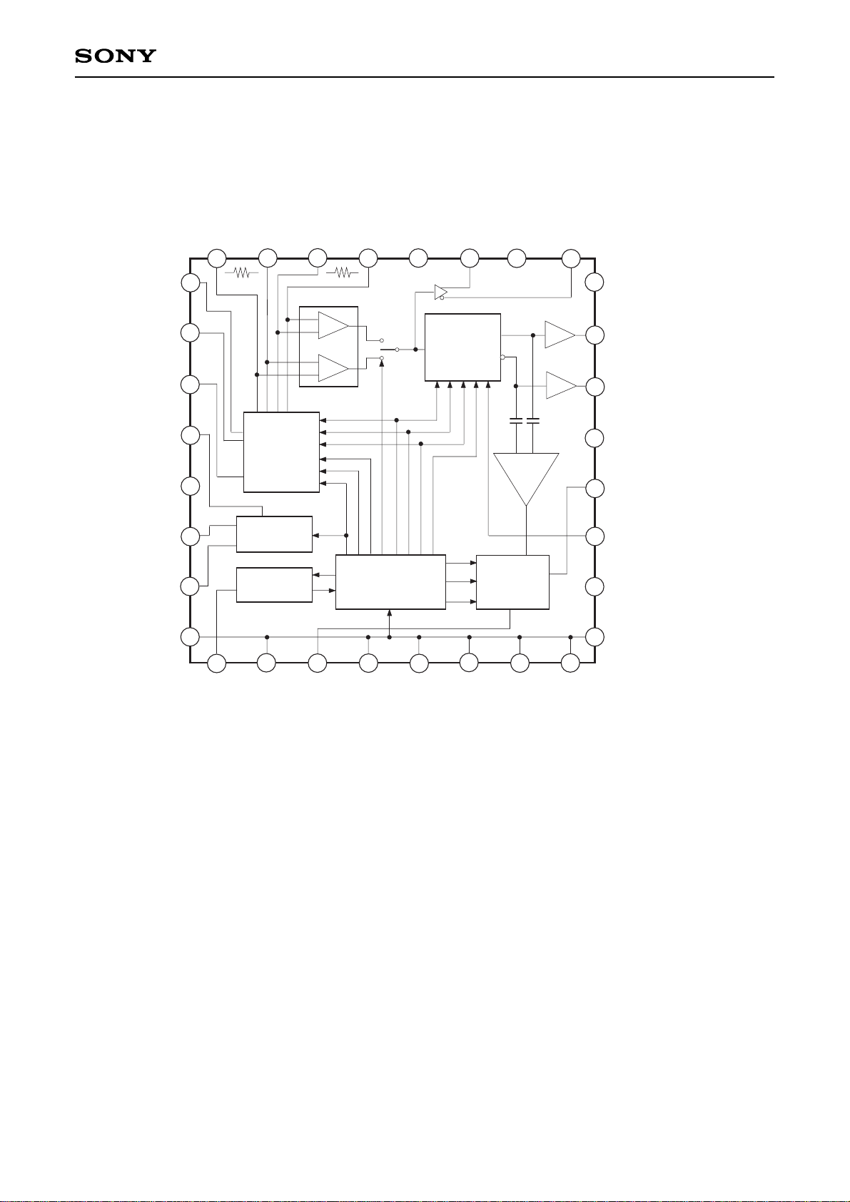
Block Diagram and Pin Configuration
XHD
FILTER
MMVA
FCSET
A.GND
HEAD0A
HEAD0B
HEAD1B
HEAD1A
PREOUTA
XWD
RD
XWG
XEG
XS1
XCI
FILTER
OUTA
OUTB
XPS
ERA1
ERA0
D.GND
POWER ON
WCLD
WCMD
IESET
XHG
PREOUTB
VCC
NC
OTF
X360
WCHD
WRITE
DRIVER
ERASE
DRIVER
POWER
MONITOR
CONTROL
LOGIC
COMP
TIME
DOMAIN
FILTER
PREAMP
FILTER
DIFF + LPF
(BPF)
2
3
4
5
6
7
8
9
10
11
12
13
14
15
16
17
18
19
20
21
22
23
24
25
26
27
28
29
30
31
32
1
– 3 –
CXA3031Q
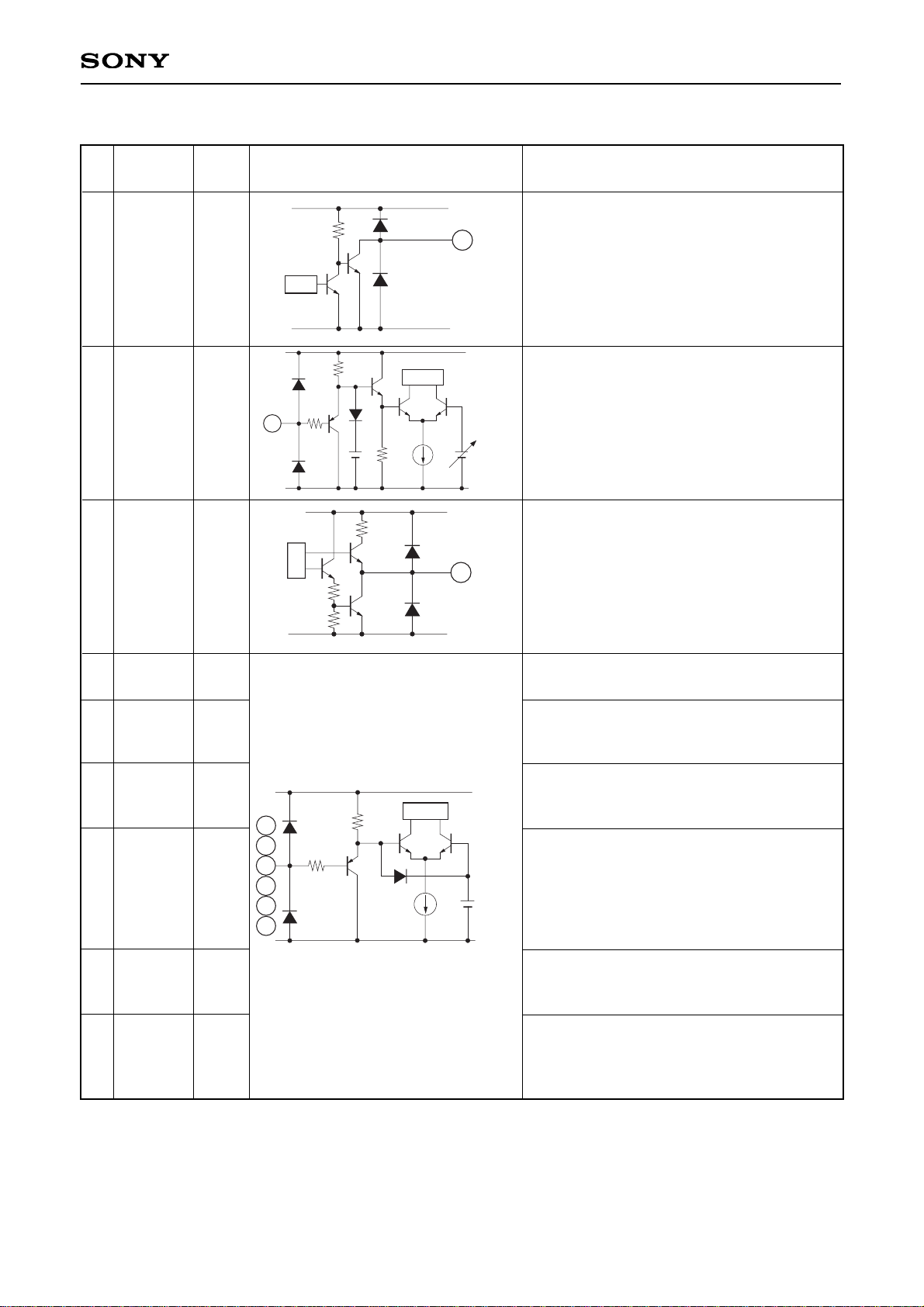
Pin Description
Pin
No.
Symbol
Pin
voltage
Equivalent circuit Description
1
POWER
ON
—
Reduced voltage detection output.
This is an open collector pin that outputs a
low signal when VCC is below the specified
value.
VCC
A.GND
100k
1
2 XWD —
Write data input.
This pin is a Schmitt-type input that is
triggered when the logical voltage goes from
High to Low.
VCC
1k
A.GND
2.3V
2
3 RD —
4 XCI —
5 XWG —
6 XEG —
7 XS1 —
8 OTF —
9 XHD —
Read data output.
This pin is active when the logical voltage of
the write gate signal and the erase gate
signal is High.
Write current control. The write current
increases when the logical voltage is Low.
Write gate signal input. The write system
becomes active when the logical voltage is
Low.
Erase gate signal input. The erase system
becomes active when the logical voltage is
Low.
Head side switching signal input. The
HEAD1 system is active when the logical
voltage is Low, and the HEAD0 system is
active when the logical voltage is High, but
only when the logical voltage for the write
gate and the erase gate is High.
Filter inner track/outer track mode control.
Inner track mode is selected when the
logical voltage is Low.
Filter, time domain filter and write current
1M/2M mode control. 2M mode is selected
when the logical voltage is Low.
140
V
CC
D.GND
3
VCC
100k
1k
A.GND
2.1V
4
5
6
7
8
9

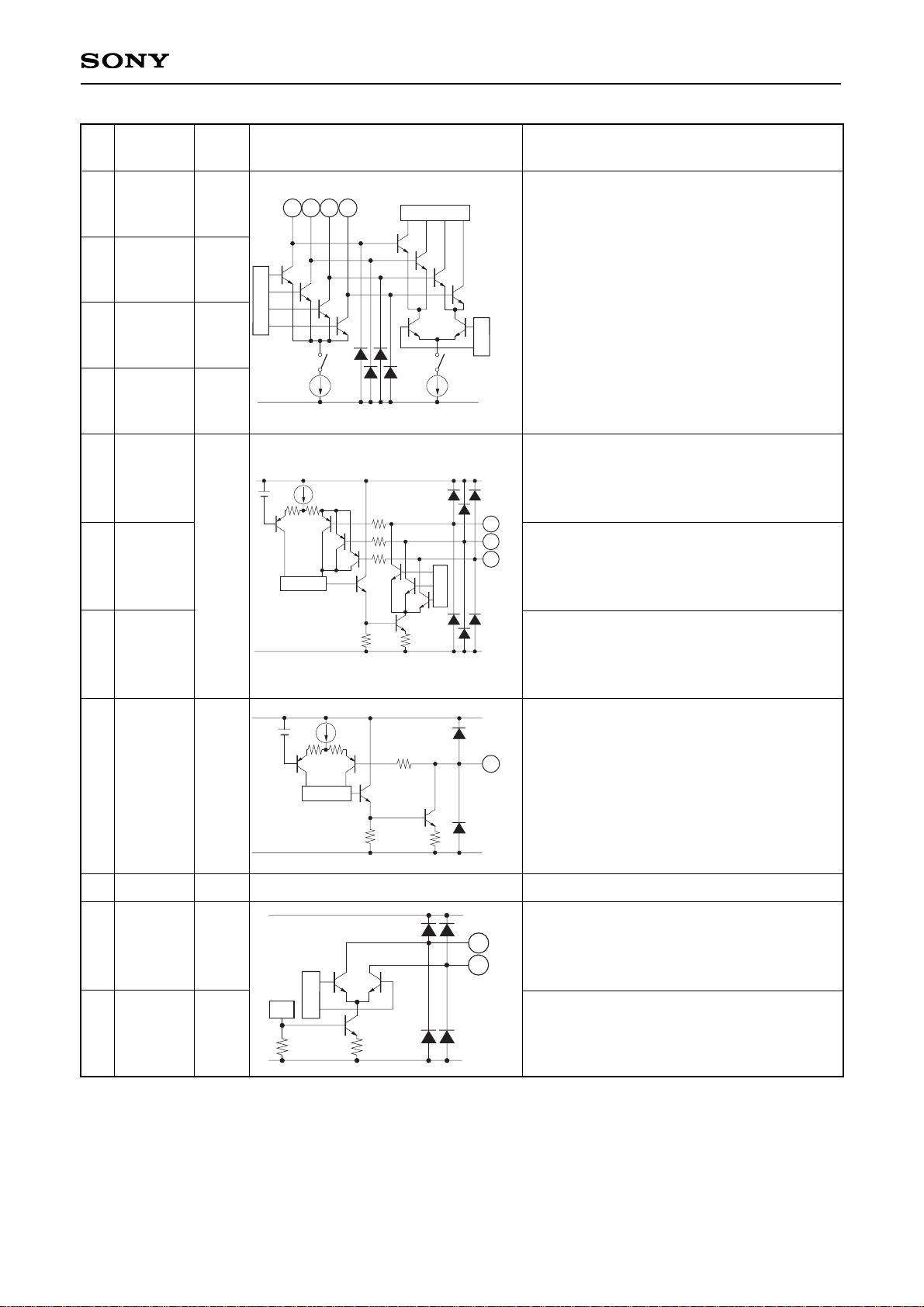
– 4 –
CXA3031Q
Pin
No.
Symbol
Pin
voltage
Equivalent circuit Description
18 X360 —
Filter, time domain filter and write current
1M/1.6M mode control. 1.6M mode is
selected when the logical voltage is Low.
18
20
VCC
100k
1k
A.GND
2.1V
VCC
A.GND
1.2V
11
1k
147
147
VCC
A.GND
1.2V
12
140
V
CC
A.GND
300µ
140
300µ
14
15
140
V
CC
A.GND
200µ
140
200µ
17
19
20 XHG
—
Preamplifier voltage gain selection. Gain is
boosted by 6dB when the logical voltage is
Low compared to when the logical voltage is
High.
10 VCC
—
Power supply (5V) connection.
11 FCSET
3.8V
Filter cutoff frequency setting resistor
connection. Connect the filter cutoff
frequency setting resistor RF between this
pin and VCC in order to set the cutoff
frequency.
12 MMVA
0.5V
Time domain filter 1st monostable
multivibrator pulse width setting. Connect
the 1st monostable multivibrator pulse width
setting resistor RA between this pin and
A.GND.
13 A.GND
—
Analog system GND connection.
14
FILTER
OUTB
3.4V
15
FILTER
OUTA
3.4V
17
PRE
OUTB
3.4V
Filter differential outputs.
19
PRE
OUTA
3.4V
Preamplifier differential outputs.
16 (NC) Not connected.
– 5 –
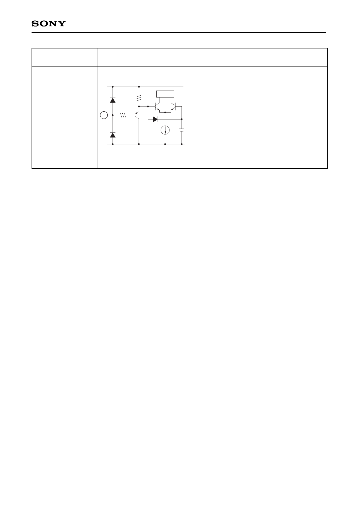
CXA3031Q
Pin
No.
Symbol
Pin
voltage
Equivalent circuit Description
21 HEAD 1B —
22 HEAD 1A —
23 HEAD 0B —
24 HEAD 0A —
25 WCLD
26 WCMD
27 WCHD
5V
when
XWG
= High
3.8V
when
XWG
= Low
28 IESET
29 D.GND
—
30 ERA0
—
31 ERA1
—
Magnetic head input/output connections.
Connect the recording/playback magnetic
head to these pins, and connect the center
tap to VCC. When the logical voltage for
Pin 7 (XS1) is Low, the HEAD1 system is
active; when the logical voltage is High, the
HEAD0 system is active.
1M write current setting resistor connection.
Connect the write current setting resistor
RWLD between this pin and VCC to set the
write current.
1.6M write current setting resistor connection.
Connect the write current setting resistor
RWMD between this pin and VCC to set the
write current.
2M write current setting resistor connection.
Connect the write current setting resistor
RWHD between this pin and VCC to set the
write current.
Erase current setting resistor connection.
Connect the erase current setting resistor RE
between this pin and VCC to set the erase
current.
Digital system GND connection.
Erase current connection for the HEAD0
system.
Erase current connection for the HEAD1
system.
A.GND
21
22
23
24
VCC
A.GND
1.2V
147
147
147
25
26
27
VCC
A.GND
1.2V
147
28
VCC
A.GND
30
31
5V
when
XEG
= High
3.8V
when
XEG
= Low
– 6 –
CXA3031Q
Pin
No.
Symbol
Pin
voltage
Equivalent circuit Description
32 XPS
—
Power saving signal input.
When the logical voltage is Low, the IC is in
power saving mode. In power saving mode,
only the power supply on/off detector operates.
VCC
162k
1k
A.GND
2.1V
32
– 7 –
CXA3031Q
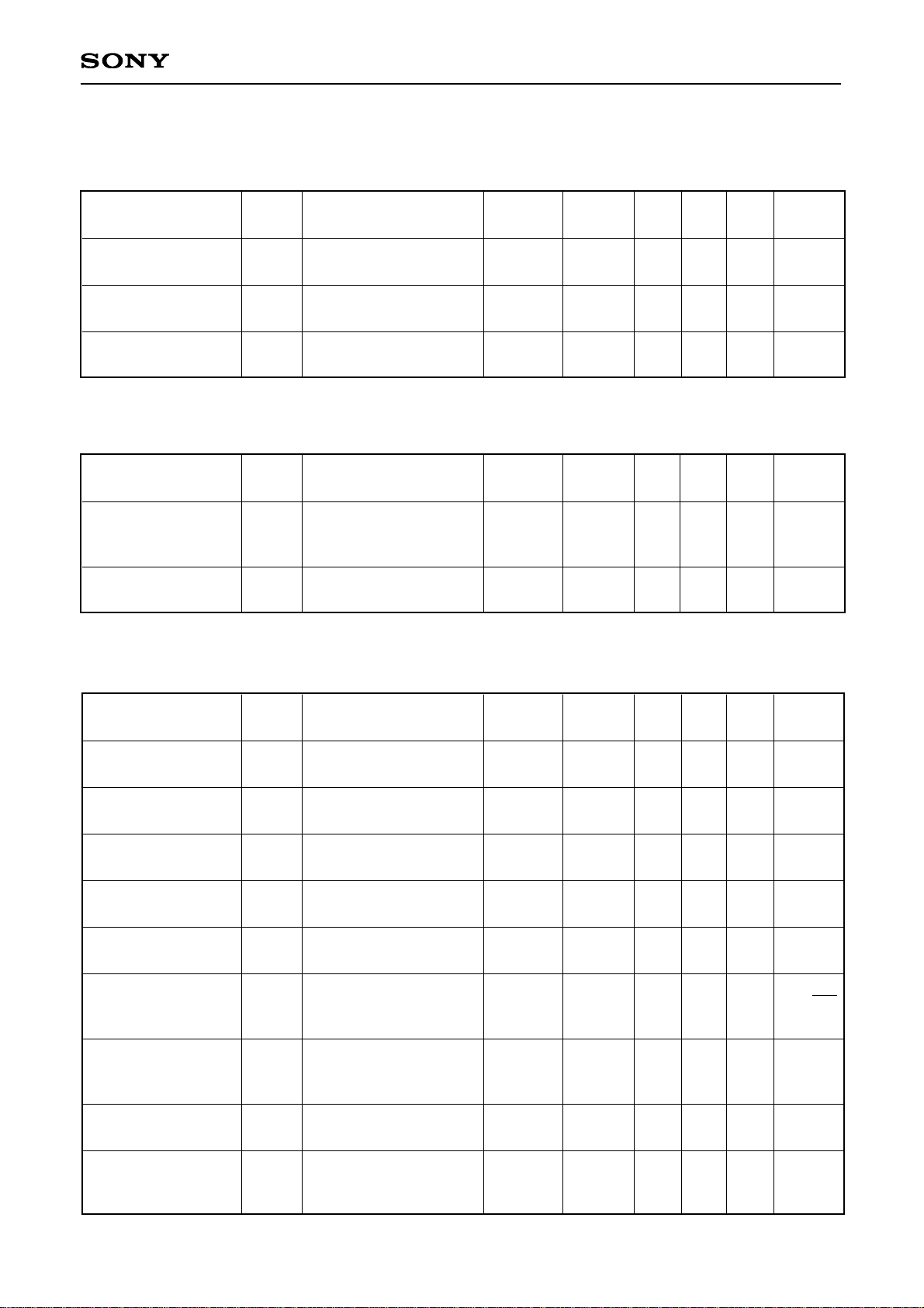
Electrical Characteristics
Current Consumption (Ta = 25°C, VCC = 5V)
Item Symbol Conditions Min. Typ. Max. Unit
Current consumption
in read mode
Current consumption
in write/erase mode
Current consumption
in power saving mode
ICCR
ICCWE
ICCPS
XWG = High
XWG = Low,
XEG = Low
XPS = Low
—
—
—
—
—
—
16
7
—
26
13
0.95
36
19
1.9
mA
mA
mA
Power Supply Monitoring System (Ta = 25°C)
Item Symbol Conditions Min. Typ. Max. Unit
Power supply on/off
detector threshold
voltage
Power on output
saturation voltage
VTH
VSP
VCC = 3.5V
I = 1mA
—
—
—
—
3.5—3.9—4.3
0.5
V
V
Read System (Ta = 25°C, VCC = 5V)
Item Symbol Conditions
Measure-
ment circuit
Measure-
ment Point
Min. Typ. Max. Unit
Preamplifier voltage gain
Low gain/outer track
Preamplifier voltage gain
Low gain/inner track
Preamplifier voltage gain
High gain/outer track
Preamplifier voltage gain
High gain/inner track
Preamplifier
frequency response
Preamplifier input
conversion noise
voltage
Preamplifier
differential output
offset voltage
Filter differential
output offset voltage
Filter differential
output voltage
amplitude
GVLO
GVLI
GVHO
GVHI
BW
EN
VOFSP
VOFSF
VOF
f = 100kHz
OTF = High, XHG = High
f = 100kHz
OTF = Low, XHG = High
f = 100kHz
OTF = High, XHG = Low
f = 100kHz
OTF = Low, XHG = Low
GV/GV (100kHz) = –3dB
Band Width
= 400Hz to 1MHz, VI = 0
VI = 0
VI = 0
1
1
1
1
1
1
1
1
1
D, E
D, E
D, E
D, E
D, E
D, E
D, E
B, C
B, C
37.1
40.1
43.1
46.1
5
—
–500
–100
2.8
39.0
42.0
45.0
48.0
—
2.0
—
—
—
40.6
43.6
46.6
49.6
—
2.9
+500
+100
—
dB
dB
dB
dB
MHz
nV/√ Hz
mV
mV
Vp-p
Measure-
ment circuit
Measure-
ment Point
Measure-
ment circuit
Measure-
ment Point
– 8 –
CXA3031Q
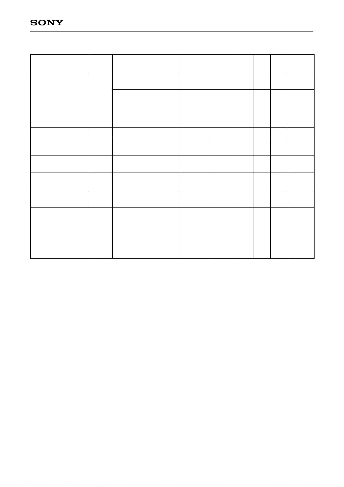
Read System (Ta = 25°C, VCC = 5V)
Time domain filter
monostable
multivibrator pulse
width
Read data pulse width
Read data output low
output voltage
Read data output
high output voltage
Read data output
∗1
rise time
Read data output
∗1
fall time
Peak shift
∗2
T1
T2
VOL
VOH
tr
tf
PS
X360 = X, XHD = High
(1M mode)
X360 = Low, XHD = Low
(1.6M mode)
or
X360 = High, XHD = Low
(2M mode) Refer to Fig. 1
Refer to Fig. 1
IOL = 2mA
IOH = –0.4mA
RL = 2kΩ
CL = 20pF
RL = 2kΩ
CL = 20pF
VI = 0.25mVp-p to
3.5mVp-p
XHG = Low, XHD = Low
OTF = Low, X360 = High
f = 125kHz, 2M/
inner track mode
Refer to Fig. 1
1
1
1
1
1
1
1
1
A, F
A, F
A
A
A
A
A
A
2.25
1.13
260
—
2.8
—
—
—
2.5
1.25
400
—
—
—
—
—
2.75
1.38
540
0.5
—
100
100
1
µs
µs
ns
V
V
ns
ns
%
∗1
Read data output: 0.5V to 2.4V
∗2
Signal input level
Low gain/outer track: VI = 0.5mVp-p to 10mVp-p
Low gain/inner track: VI = 0.5mVp-p to 7mVp-p
High gain/outer track: VI = 0.25mVp-p to 5mVp-p
High gain/inner track: VI = 0.25mVp-p to 3.5mVp-p
Item Symbol Conditions Min. Typ. Max. Unit
Measure-
ment circuit
Measure-
ment Point
 Loading...