

Sony CXA3026AQ Datasheet
—1—
E96304C92
Sony reserves the right to change products and specifications without prior notice. This information does not convey any license by
any implication or otherwise under any patents or other right. Application circuits shown, if any, are typical examples illustrating the
operation of the devices. Sony cannot assume responsibility for any problems arising out of the use of these circuits.
Structure
Bipolar silicon monolithic IC
Applications
• Magnetic recording (PRML)
• Communications (QPSK, QAM)
• LCDs
• Digital oscilloscopes
Description
The CXA3026AQ is an 8-bit high-speed flash A/D
converter capable of digitizing analog signals at the
maximum rate of 140MSPS. ECL, PECL or TTL can
be selected as the digital input level in accordance
with the application. The TTL digital output level
allows 1:2 demultiplexed output.
Features
• Differential linearity error: ±0.5LSB or less
• Integral linearity error: ±0.5LSB or less
• High-speed operation with a maximum
conversion rate of 140MSPS
• Low input capacitance: 21 pF
• Wide analog input bandwidth: 150 MHz
• Low power consumption: 790 mW
• Low error rate
• Excellent temperature characteristics
• 1:2 demultiplexed output
• 1/2 frequency divided clock output
(with reset function)
• Compatible with ECL, PECL and TTL digital input
levels
• Single +5 V power supply operation available
• Surface mounting package
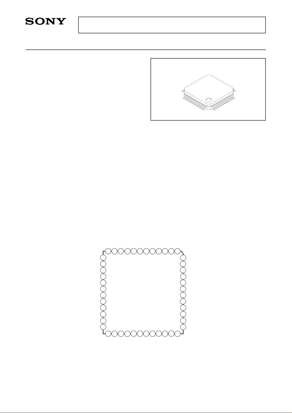
Pin Configuration (Top View)
8-bit 140MSPS Flash A/D Converter
48 pin QFP (Plastic)
CXA3026AQ
LEAD TREATMENT: PALLADIUM PLATING
CLK/E
N.C.
CLK/T
N.C.
N.C.
DV
CC2
DGND2
P2D0
P2D1
P2D2
P2D3
CLKN/E
P2D4
P2D7
P2D6
DGND1
DV
CC
1
DV
CC
2
DGND2
P1D0
P1D1
P1D2
P1D3
P2D5
RESETN/E
SELECT
RESETN/T
INV
CLKOUT
DV
CC2
DGND2
P1D7
P1D6
P1D5
P1D4
RESET/E
DV
EE
3
V
RM
1
AGND
AV
CC
V
IN
V
RM
2
AV
CC
V
RM
3
AGND
V
RT
DGND3
V
RB
13
14
15
16
17
18
19
20
21
22
23
24
25
26
27
28
29
30
40
39
38
37
36
35
34
31
32
33
41
42
43
44
45
46
47
48
2
3
4
5
6
7
8
9
10
11
12 1

—2—
CXA3026AQ
Absolute Maximum Ratings (Ta = 25 °C)
Unit
• Supply voltage AVCC, DVCC1, DVCC2 –0.5 to +7.0 V
DGND3 –0.5 to +7.0 V
DVEE3 –7.0 to +0.5 V
DGND3 – DVEE3 –0.5 to +7.0 V
• Analog input voltage VIN VRT – 2.7 to AVCC V
• Reference input voltage VRT 2.7 to AVCC V
VRB VIN – 2.7 to AVCC V
|VRT – VRB| 2.5 V
• Digital input voltage ECL (∗∗∗/E∗1) DVEE3 to +0.5 V
PECL (∗∗∗/E) –0.5 to DGND3 V
TTL (∗∗∗/T, INV) –0.5 to DVCC1 V
other (SELECT) –0.5 to DVCC1 V
VID∗2(|∗∗∗/E – ∗∗∗N/E|) 2.7 V
• Storage temperature Tstg –65 to +150 °C
• Allowable power dissipation PD 2 W
(when mounted on a glass fabric base epoxy board with 50mm x 50mm, 1.6mm thick)
Recommended Operating Conditions
With a single power supply With dual power supplies Unit
Min. Typ. Max. Min. Typ. Max.
• Supply voltage DVCC1, DVCC2, AVCC +4.75 +5.0 +5.25 +4.75 +5.0 +5.25 V
DGND1, DGND2, AGND –0.05 0 +0.05 –0.05 0 +0.05 V
DGND3 +4.75 +5.0 +5.25 –0.05 0 +0.05 V
DVEE3 –0.05 0 +0.05 –5.5 –5.0 –4.75 V
• Analog input voltage VIN VRB VRT VRB VRT V
• Reference input voltage VRT +2.9 +4.1 +2.9 +4.1 V
VRB +1.4 +2.6 +1.4 +2.6 V
|VRT – VRB| 1.5 2.1 1.5 2.1 V
• Digital input voltage ECL (∗∗∗/E) : VIH DGND3 – 1.05 DGND3 – 0.5 V
: VIL DGND3 – 3.2 DGND3 – 1.4 V
PECL (∗∗∗/E) : VIH DGND3 – 1.05 DGND3 – 0.5 V
: VIL DGND3 – 3.2 DGND3 – 1.4 V
TTL (∗∗∗/T, INV) : VIH 2.0 2.0 V
: VIL 0.8 0.8 V
other (SELECT) : VIH DVCC1 DVCC1 V
: VIL DGND1 DGND1 V
VID∗2(|∗∗∗/E – ∗∗∗N/E|) 0.4 0.8 0.4 0.8 V
•
Maximum conversion rate
Fc (Straight mode) 100 100 MSPS
(DMUX mode) 140 140 MSPS
• Ambient temperature Ta –20 +75 –20 +75 °C
∗1∗∗∗/E and ∗∗∗/T indicate CLK/E and CLK/T, etc. for the pin name.
∗2VID: Input Voltage Differential
ECL and PECL switching level
VID
V
IL (min.)
V
IH
VTH (DGND3–1.2V)
V
IL
VIH (max.)
DGND3
—3—
CXA3026AQ
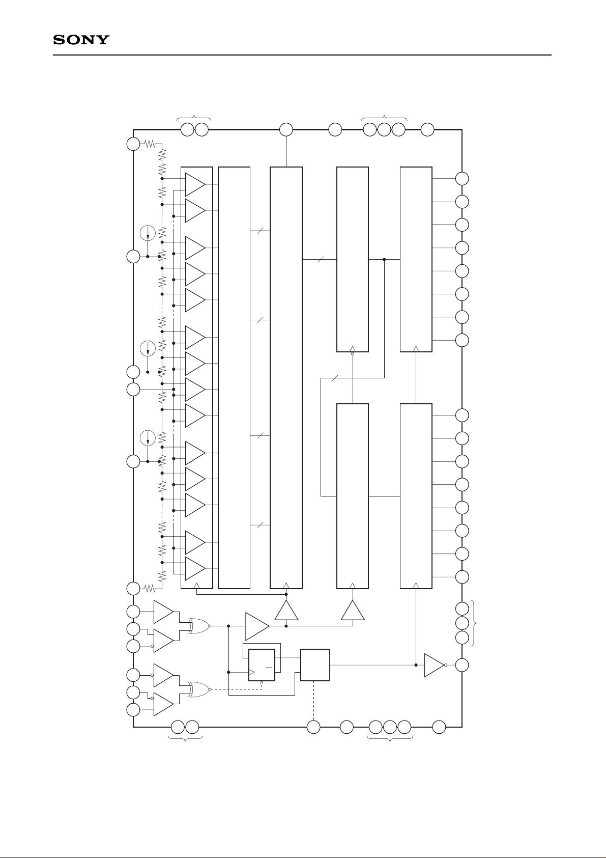
Block Diagram
6bits
VRT
2
3
5
8
10
12
13
14
16
17
18
19
20
21
22
23
24
25
26
27
28
29
30
40
39
38
37
36
35
34
31
32
33
41
42
44
1
1
2
r/2
63
64
•
•
•
65
126
127
128
129
191
192
•
•
•
193
254
255
•
•
•
r
6bits
9
7
4
r1
r2
r
r
r
r
r
r
r
r
r
r
r
r
r
r
/2
6bits
6bits
8bits
8bits
Delay
15
46
47
48
Select
D Q
Q
45
SELECT
11
43
DGND1 DVEE3
DGND2
AGND
AVCC DVCC2
DV
CC1INV DGND3
VRM3
VIN
VRM2
6
V
RB
VRM1
CLK/T
CLK/E
CLKN/E
RESETN/T
RESETN/E
RESET/E
CLKOUT
N. C.
P2D0
P2D1
P2D2
P2D3
P2D4
P2D5
P2D6
P2D7
P1D0
P1D1
P1D2
P1D3
P1D4
P1D5
P1D6
P1D7
TTL OUT
LATCH B
TTL OUT
LATCH A
6-bit LATCH+ENCODER
ENCODER
(LSB)
(MSB)
(LSB)
(MSB)
•
•
•
—4—
CXA3026AQ
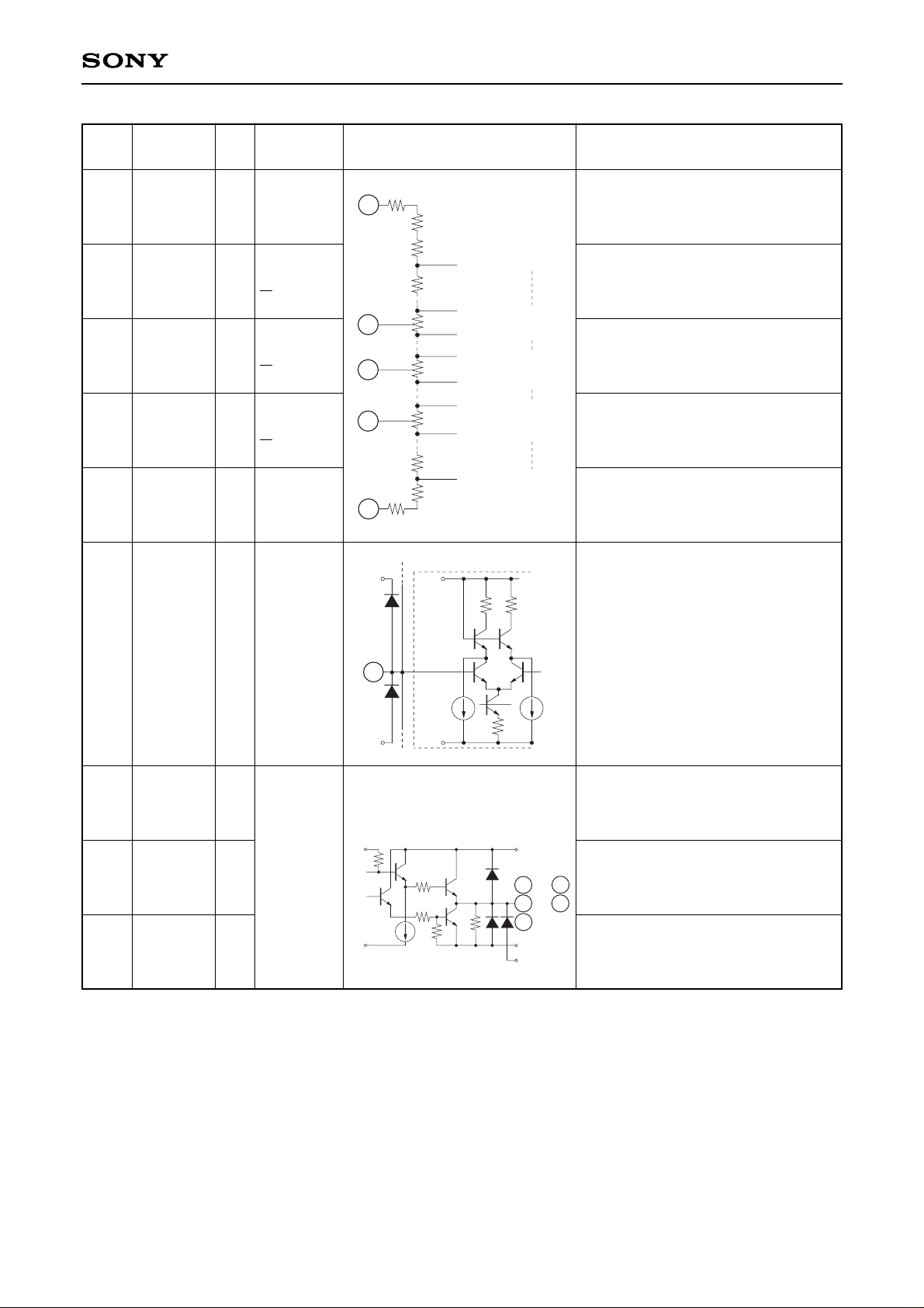
Pin Description and I/O Pin Equivalent Circuit
Analog ground.
Separated from the digital ground.
Analog power supply.
Separated from the digital power
supply.
Digital ground.
Digital power supply.
Digital power supply.
Ground for ECL input.
+5 V for PECL and TTL input.
Digital power supply.
–5 V for ECL input.
Ground for PECL and TTL input.
No connected pin.
Not connected with the internal
circuits.
Clock input.
CLK/E complementary input.
When left open, this pin goes to the
threshold potential.
Only CLK/E can be used for
operation, but complementary input
is recommended to attain fast and
stable operation.
Reset input.
When the input is set to low level,
the built-in CLK frequency divider
circuit can be reset.
RESETN/E complementary input.
When left open, this pin goes to the
threshold voltage. Only RESETN/E
can be used for operation.
3, 10
5, 8
20, 29
32, 41
19, 30
31, 42
12
1
16, 17
18
13
14
48
47
AGND
AVCC
DGND1
DGND2
DVCC1
DVCC2
DGND3
DVEE3
N.C.
CLK/E
CLKN/E
RESETN/E
RESET/E
GND
+5 V
(typ.)
GND
+5 V
(typ.)
+5 V (Typ.)
(With a
single
power
supply)
GND
(With dual
power
supplies)
GND
(With a
single
power
supply)
–5 V (Typ.)
(With dual
power
supplies)
ECL/
PECL
Pin
No.
Symbol
I
I
I
I
I/O
Standard
voltage level
Equivalent circuit Description
DGND3
DV
EE3
r r
1.2V
r
r
13
14
48
47
—5—
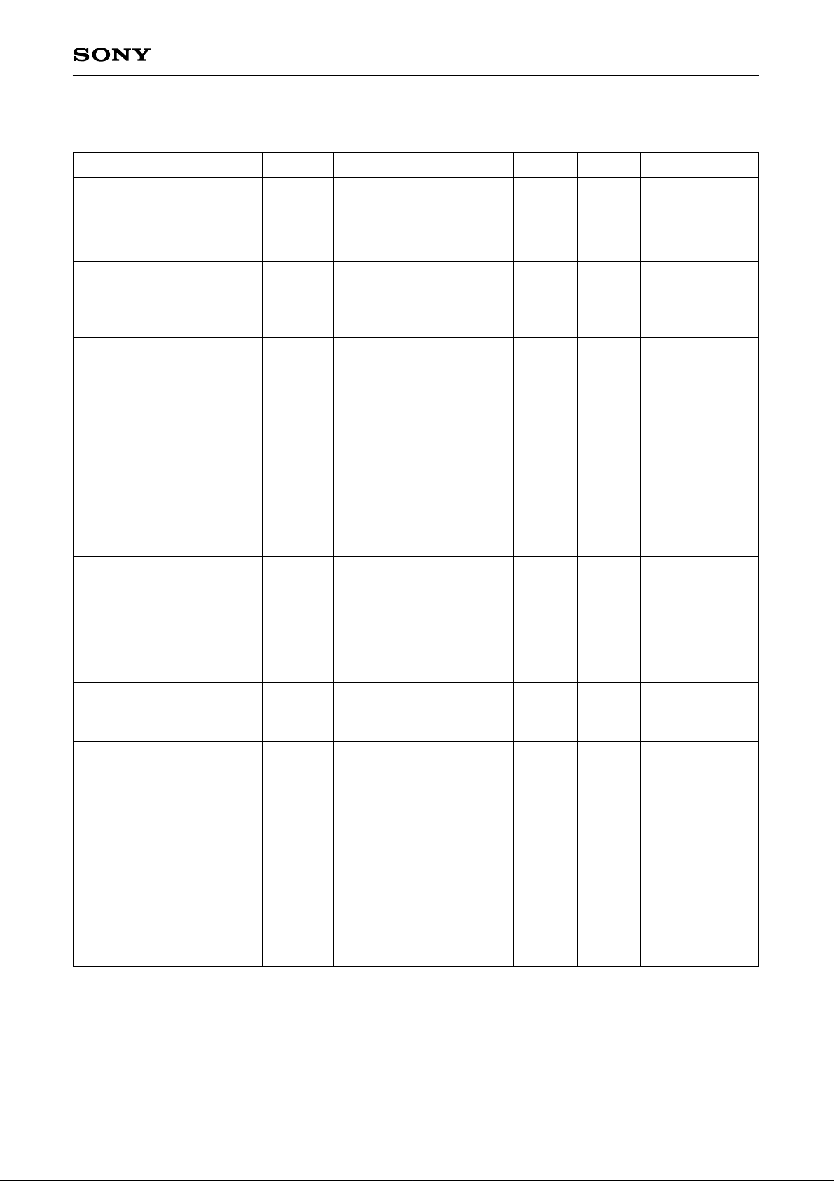
CXA3026AQ
15 CLK/T
Clock input.
46
RESETN/T
TTL
TTL
VCC
or
GND
Reset input.
When left open, this input goes to
high level. When the input is set to
low level, the built-in CLK frequency
divider circuit can be reset.
44
INV
Data output polarity inversion input.
When left open, this input goes to
high level.
(See Table 1. I/O Correspondence
Table.)
45
SELECT
Data output mode selection.
(See Table 2. Operating Mode
Table.)
DVCC1
DGND1
1.5V
r/2
r
DVEE3
15
46
DVCC1
DGND1
DVEE3
44
DVCC1
DGND1
DVEE3
45
I
I
I
Pin
No.
Symbol I/O
Standard
voltage level
Equivalent circuit Description
—6—
CXA3026AQ
Pin
Symbol I/O
Standard
Equivalent circuit Description
No.
voltage level
11
9
7
4
2
6
33
to
40
21
to
28
43
VRT
VRM3
VRM2
VRM1
VRB
VIN
P1D0
to
P1D7
P2D0
to
P2D7
CLKOUT
I
I
I
O
O
O
4.0 V
(typ.)
VRB +
3
(VRT – VRB)
4
VRB +
2
(VRT – VRB)
4
VRB +
1
(VRT – VRB)
4
2.0 V
(typ.)
VRT
to
VRB
TTL
Top reference voltage.
By-pass to AGND with a 1 µF tantal
capacitor and a 0.1 µF chip capacitor.
Reference voltage mid point.
By-pass to AGND with a 0.1 µF chip
capacitor.
Reference voltage mid point.
By-pass to AGND with a 0.1 µF chip
capacitor.
Reference voltage mid point.
By-pass to AGND with a 0.1 µF chip
capacitor.
Bottom reference voltage.
By-pass to AGND with a 1 µF tantal
capacitor and a 0.1 µF chip capacitor.
Analog input.
Port 1 side data output.
Port 2 side data output.
Clock output.
(See Table 2. Operating Mode Table.)
r1
r/2
Comparator 1
Comparator 63
Comparator 64
Comparator 128
Comparator 191
Comparator 127
Comparator 192
Comparator 255
r
r
2
r/2
r
r
r
r
4
7
9
2
11
r
AVCC
Comparator
AVCC
6
Vref
DVEE3
DVCC1
DGND1
AGND
DVCC2
100K
DGND2
DVEE3
to
28
21
to
40
33
43
—7—
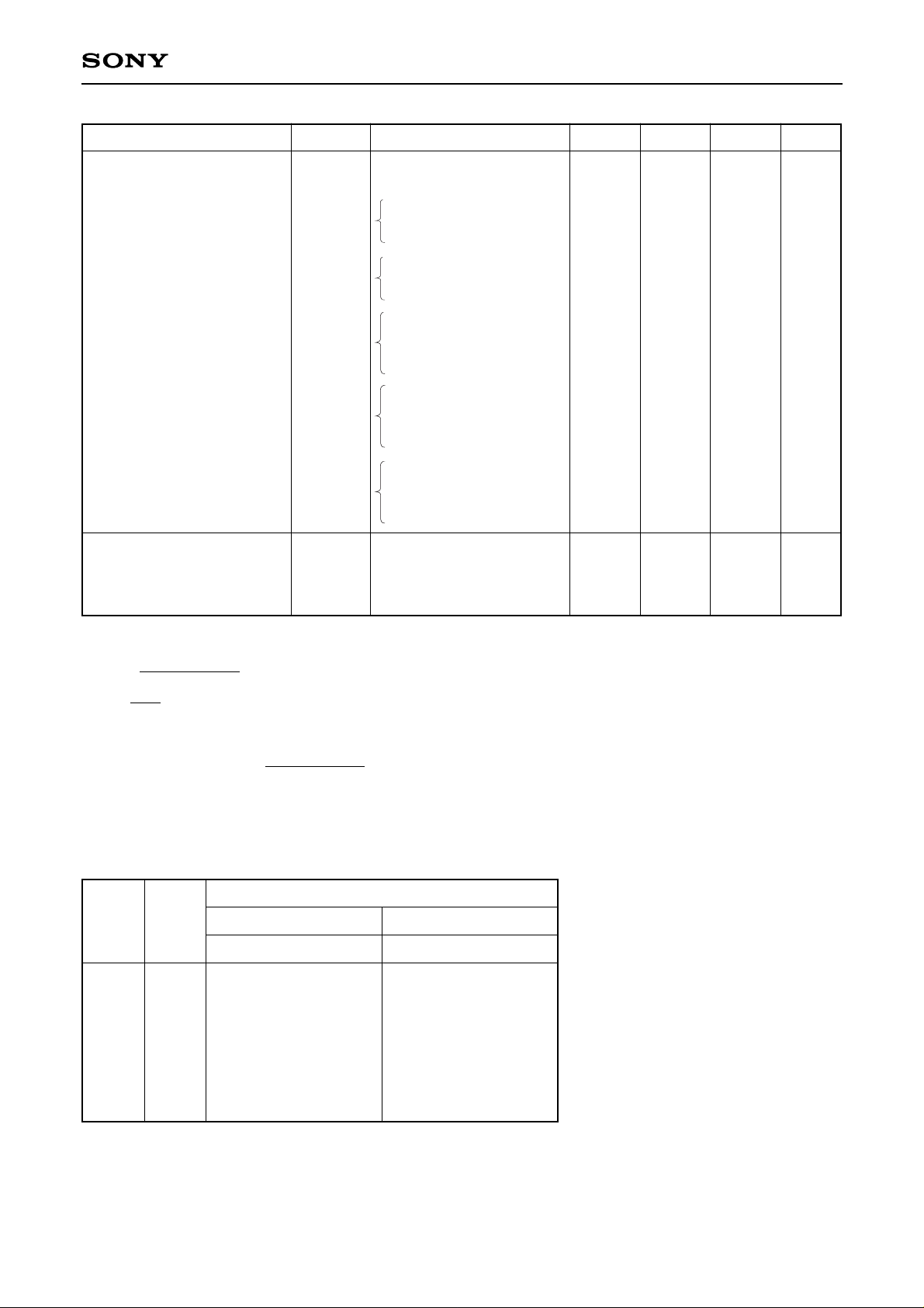
CXA3026AQ
Resolution
DC characteristics
Integral linearity error
Differential linearity error
Analog input
Analog input capacitance
Analog input resistance
Analog input current
Reference input
Reference resistance
Reference current
Offset voltage VRT side
VRB side
Digital input (ECL, PECL)
Digital input voltage: High
: Low
Threshold voltage
Digital input current: High
: Low
Digital input capacitance
Digital input (TTL)
Digital input voltage: High
: Low
Threshold voltage
Digital input current: High
: Low
Digital input capacitance
Digital output (TTL)
Digital output voltage
: High
: Low
Switching characteristics
Maximum conversion rate
Aperture jitter
Sampling delay
Clock high pulse width
Clock low pulse width
RESET Signal setup time
RESET Signal hold time
CLKOUT output delay
Data output delay
Output rise time
Output fall time
Electrical Characteristics
(DVCC1, 2, AVCC, DGND3 = +5 V, DGND1, 2, AGND, DVEE3 = 0 V, VRT = 4 V, VRB = 2 V, Ta = 25 °C)
Item Symbol Min. Typ. Max. UnitConditions
EIL
EDL
CIN
RIN
IIN
Rref
∗3
Iref
∗4
EOT
EOB
VIH
VIL
VTH
IIH
IIL
VIH
VIL
VTH
IIH
IIL
VOH
VOL
Fc
Taj
Tds
Tpw1
Tpw0
T_rs
T_rh
Td_clk
Tdo1
Tdo2
Tr
Tf
4
0
75
9.7
2
2
DGND3 – 1.05
DGND3 – 3.2
–50
–75
2.0
–50
–500
2.4
140
3
3.0
3.0
3.5
0
4.5
T
∗5
6.5
8
21
115
17.4
DGND3 – 1.2
1.5
10
4.5
7
T + 1
8
2
2
±0.5
±0.5
50
500
155
28
15
10
DGND3 – 0.5
DGND3 – 1.4
+50
0
5
0.8
0
0
5
0.5
6
8
T + 2
10
bits
LSB
LSB
pF
kΩ
µA
Ω
mA
mV
mV
V
V
V
µA
µA
pF
V
V
V
µA
µA
pF
V
V
MSPS
ps
ns
ns
ns
ns
ns
ns
ns
ns
ns
ns
VIN = 2 Vp-p, Fc = 5MSPS
VIN = +3.0 V + 0.07 Vrms
VIH = DGND3 – 0.8 V
VIL = DGND3 – 1.6 V
VIH = 3.5 V
VIL = 0.2 V
IOH = –2 mA
IOL = 1 mA
DMUX mode
CLK
CLK
RESETN – CLK
RESETN – CLK
(CL = 5 pF)
DMUX mode (CL = 5 pF)
(CL = 5 pF)
0.8 to 2.0 V (CL = 5 pF)
0.8 to 2.0 V (CL = 5 pF)
∗These characteristics are for PECL input,unless otherwise specified.
—8—
CXA3026AQ
∗
5
T =
∗
6
TPS: Times Per Sample
∗
7
Pd = (ICC + IEE) VCC +
(VRT – VRB)
2
Rref
Table 1. I/O Correspondence Table
Dynamic characteristics
Input bandwidth
S/N ratio
Error rate
Power supply
Supply current
Supply current
Power consumption
ICC
IEE
Pd
∗
7
150
110
0.4
570
46
40
150
0.6
790
10
–12
10
–9
10
–9
180
0.8
960
MHz
dB
dB
TPS
∗
6
TPS
TPS
mA
mA
mW
VIN = 2 Vp-p, –3 dB
Fc = 140MSPS,
fin = 1 kHz Fs
DMUX mode
Fc = 140MSPS,
fin = 34.999 MHz Fs
DMUX mode
Fc = 140MSPS,
fin = 1 kHz Fs
DMUX mode
Error>16LSB
Fc = 140MSPS,
fin = 34.999 MHz Fs
DMUX mode
Error>16LSB
Fc = 100MSPS,
fin = 24.999 MHz Fs
Straight mode
Error>16LSB
1
Fc
INV
1
D7 D0 D7 D0
0
VIN
VRT
VRM2
VRB
255
254
128
127
1
0
1 1 1 1 1 1 1 1
1 1 1 1 1 1 1 0
1 0 0 0 0 0 0 0
0 1 1 1 1 1 1 1
0 0 0 0 0 0 0 1
0 0 0 0 0 0 0 0
0 0 0 0 0 0 0 0
0 0 0 0 0 0 0 1
0 1 1 1 1 1 1 1
1 0 0 0 0 0 0 0
1 1 1 1 1 1 1 0
1 1 1 1 1 1 1 1
Step
Item Symbol Min. Typ. Max. UnitConditions
∗
3
Rref: Resistance value between VRT and VRB
∗
4
Iref =
VRT – VRB
Rref
……
……
……
—9—
CXA3026AQ
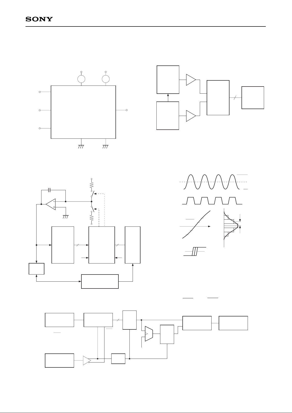
Electrical Characteristics Measurement Circuit
Current Consumption Measurement Circuit
VRT
VIN
VRB
AVCC
DVCC1
DVCC2
DGND3
DGND2
DGND1
AGND
CLK/E
DV
EE3
A A
5MHz PECL
4V
1.95V
2V
5V 5V
Icc
I
EE
Integral Linearity Error Measurement Circuit
Differential Linearity Error Measurement Circuit
CXA3026AQ
A<B A>B
Comparator
Buffer
Controller
DVM
8 8
"1""0"
000…00
to
111…10
V
IN
+V
–V
S2
S1
S1 : ON when A<B
S2: ON when A>B
B8
to
B1
B0
A8
to
A1
A0
Sampling Delay Measurement Circuit
Aperture Jitter Measurement Circuit
CXA3026AQ
OSC2
Logic
Analizer
100MHz
100MHz
Amp
ECL
Buffer
CLK
V
IN
8
fr
1024
samples
OSC1
: Variableφ
Aperture Jitter Measurement Method
VIN
CLK
V
IN
CLK
VRT
VRM2
V
RB
129
128
127
126
125
Sampling timing fluctuation
(= aperture jitter)
σ (LSB)
t∆υ∆
Error Rate Measurement Circuit
Comparator
A>B
Pulse
Counter
CXA3026AQ
Signal
Source
Latch
Latch
1 / 8
+
Signal
Source
Fc
4
–1kHz
2Vp-p Sin Wave
Fc
V
IN
CLK CLK
8
16LSB
A
B
Where σ(LSB) is the deviation of the output codes when
the largest slew rate point is sampled at the clock which
has exactly the same frequency as the analog input
signal, the aperture jitter Taj is:
Taj = σ / = σ/ ( )
∆t
∆υ
2
256
× 2 πf
 Loading...