

Sony CXA3025N Datasheet
All Band TV Tuner IC (VHF-CATV-UHF)
Description
The CXA3025N is a single chip TV tuner IC which
performs as a mixer, oscillator for UHF and VHFCATV bands. An IF amplifier is also provided.
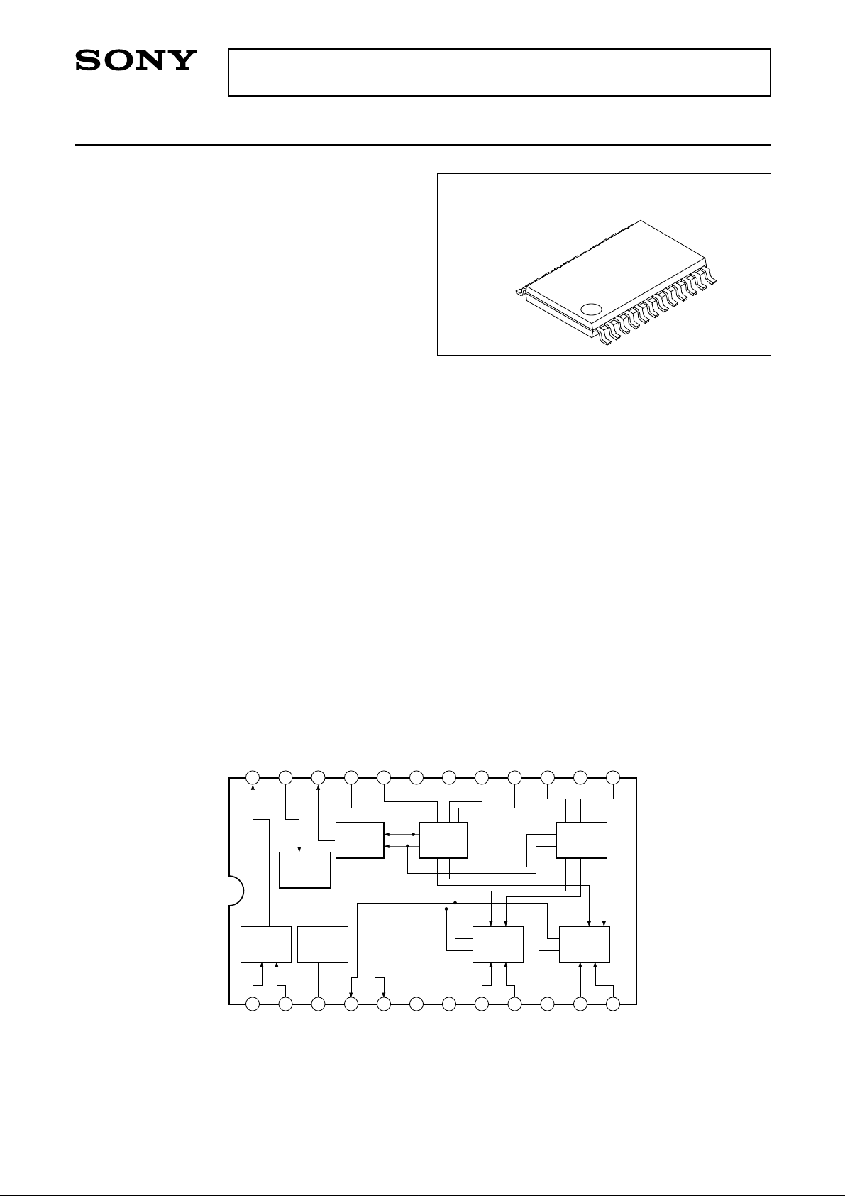
This IC adopts a 24-pin SSOP package (0.8mm
pitch) in response to the trend towards miniaturizing
the tuner and automatic IC mounting.
Features
• Low noise figure
• Superior cross modulation
• Low spurious
• Stable oscillating characteristics
• Local oscillator output for PLL
• Double tune filter connectable to MIX output
• Low thermal resistance package
Absolute Maximum Ratings (Ta = 25°C)
• Supply voltage VCC 10.5 V
• Storage temperature Tstg –65 to +150 °C
• Allowable power dissipation
CXA3025N
24 pin SSOP (Plastic)
PD 1200 mW
(when mounted on a board)
Structure
Bipolar silicon monolithic IC
Applications
• TV tuner
• CATV tuner
• VCR tuner
Block Diagram and Pin Configuration (Top View)
BANDSW
IFOUT
24
IF AMP
PLLOUT
23
22
BAND
SW
REG
UOSCB2
21
OSC
BUFF
UOSCE2
20
Operating Conditions
• Supply voltage VCC 9.0 ± 0.9 V
• Operating temperature Topr –20 to +75 °C
GND
GND
19
UHF
OSC
UOSCE1
18
17
VHF
MIX
UOSCB1
16
VOSCC
15
14
VHF
OSC
UHF
MIX
NC
VOSCB
13
1
IFIN1
2
IFIN2
4
3
CC
V
MIXOUT2
MIXOUT1
GND
7
GND
6
5
8
VHFIN1
9
VHFIN2
11
UHFIN1
12
UHFIN2
10
NC
Sony reserves the right to change products and specifications without prior notice. This information does not convey any license by
any implication or otherwise under any patents or other right. Application circuits shown, if any, are typical examples illustrating the
operation of the devices. Sony cannot assume responsibility for any problems arising out of the use of these circuits.
– 1 –
E95Y06-ST
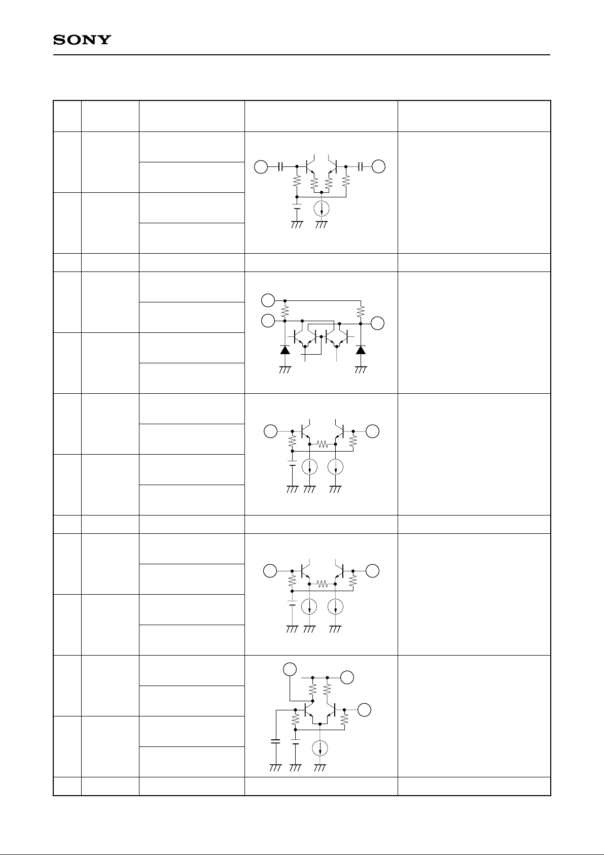
Pin Description and Equivalent Circuit
CXA3025N
Pin
No.
1
2
3
4
5
Symbol
IFIN1
IFIN2
VCC
MIXOUT1
MIXOUT2
Pin voltage
typ. (V)
During VHF reception
—
During UHF reception
—
—
—
9.0
7.4
7.2
7.4
7.2
Equivalent circuit Description
1
2
8k8k
IF amplifier inputs.
Power supply.
VCC
3
450 450
4
5
Mixer outputs.
8
9
10
11
12
13
15
VHFIN1
VHFIN2
NC
UHFIN1
UHFIN2
VOSCB
VOSCC
3.2
3.4
3.2
3.4
3.4
3.2
3.4
3.2
3.3
3.5
6.3
9.0
8
6k 6k
11
6k 6k
15
1k
3k
9
VHF inputs.
Normally a capacitor is
connected at Pin 8 to GND and
Pin 9 is used for input.
No connected.
12
UHF inputs.
Balanced input to Pins 11 and
12 or a capacitor is connected
at Pin 11 to GND and Pin 12 is
used for input.
3
VCC
13
3k
VHF oscillators.
14
NC
No connected.
– 2 –
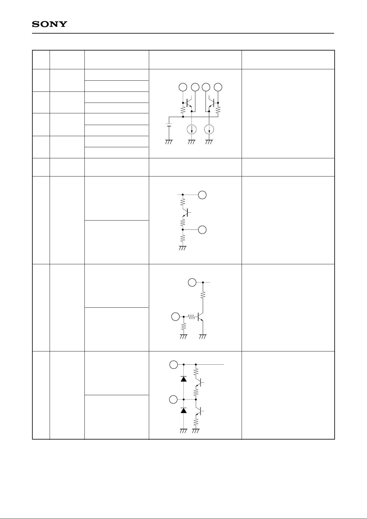
CXA3025N
Pin
No.
16
17
20
21
6, 7
18 19
22
Symbol
UOSCB1
UOSCE1
UOSCE2
UOSCB2
GND
PLLOUT
Pin voltage
typ. (V)
3.5
3.3
3.0
2.5
3.0
2.5
3.5
3.3
0
5.8
5.7
Equivalent circuit Description
20
17
16
21
UHF oscillators.
GNDs.
VCC
3
30
22
3.2k
PLL IC oscillator output.
23
24
BANDSW
IFOUT
0
3.0
Under VHF
operation : 4.5
Under UHF
operation : 4.5
24
VCC
3
900
Band switching. UHF operation
when 3V or more voltage is
1.6k
23
20k
VCC
3
47
applied externally, and VHF
operation when OPEN or 0.5V
or less voltage is applied.
IF output.
– 3 –
CXA3025N
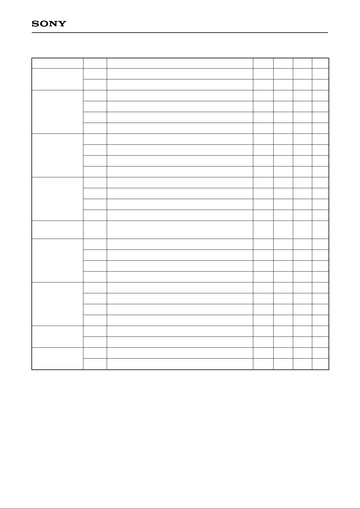
Electrical Characteristics See Electrical Characteristics Measurement Circuit. (Ta = 25°C, VCC = 9V)
Item
Circuit current
Conversion
∗1
gain
Noise figure
∗1 ∗2
1% cross
modulation
∗1 ∗3
Max. output
power
Symbol Measurement conditions Min. Typ. Max. Unit
IccV
IccU
CG1
CG2
CG3
CG4
NF1
NF2
NF3
NF4
CM1
CM2
CM3
CM4
Pomax
(sat)
VHF operation; no signal
UHF operation; no signal
VHF operation; fRF = 55MHz; Input level –40dBm
VHF operation; fRF = 360MHz; Input level –40dBm
UHF operation; fRF = 360MHz; Input level –40dBm
UHF operation; fRF = 800MHz; Input level –40dBm
VHF operation; fRF = 55MHz
VHF operation; fRF = 360MHz
UHF operation; fRF = 360MHz
UHF operation; fRF = 800MHz
VHF operation; fD = 55MHz; fUD = ±12MHz
VHF operation; fD = 360MHz; fUD = ±12MHz
UHF operation; fD = 360MHz; fUD = ±12MHz
UHF operation; fD = 800MHz; fUD = ±12MHz
50Ω load
38
37
17
18
23
23
99
97
91
89
+8
53
51
20
21
26
26
13
12
9
9
102
100
94
92
+10
63
62
23
24
29
29
16
15
13
13
mA
mA
dB
dB
dB
dB
dB
dB
dB
dB
dBµ
dBµ
dBµ
dBµ
dBm
∆fsw1
∆fsw2
Switch ON drift
∗4
∆fsw3
∆fsw4
∆fst1
+B drift
∗5
∆fst2
∆fst3
∆fst4
PLL OUT output
power
Band switch
voltage
∗1
Measured value for untuned inputs.
∗2
Noise figure is the directly-read value of the NF meter in DSB.
∗3
Desired signal (fD) input level is –33dBm. Undesired signal (fUD) is 100kHz, 30% AM at ±12MHz. The
PoscV
PoscU
VswV
VswU
VHF operation; fOSC = 100MHz
VHF operation; fOSC = 405MHz
UHF operation; fOSC = 405MHz
UHF operation; fOSC = 845MHz
VHF operation; fOSC = 100MHz
VHF operation; fOSC = 405MHz
UHF operation; fOSC = 405MHz
UHF operation; fOSC = 845MHz
VHF operation; 50Ω load
UHF operation; 50Ω load
VHF operation
UHF operation
–20
–20
0
3
±200
±300
±300
±300
±100
±200
±150
±150
–10
–10
0.5
10.5
measurement value is the undesired signal level, measured with a spectrum analyzer at S/I = 46dB.
∗4
Frequency variation from 3 seconds to 3 minutes after switch ON.
∗5
Frequency variation when VCC = 9V ± 5% variation.
kHz
kHz
kHz
kHz
kHz
kHz
kHz
kHz
dBm
dBm
V
V
– 4 –
 Loading...