

Sony CXA3003R Datasheet

CXA3003R
For the availability of this product, please contact the sales office.
Baseband analog processing IC for dual-mode CDMA/FM cellular phone
Description
The CXA3003R is a baseband analog processing
IC for dual-mode CDMA/FM cellular phone. The
CXA3003R interfaces between the inter-frequency
section and the digital processing circuitry of the
telephone. The receive circuit functions primarily
convert analog IF signals to the analog baseband
frequency range and to convert the analog
baseband signals into digital signals. Transmit
circuits convert digital data into analog baseband
signals which are then up-convert to the IF
frequency range.
Features
• Receive signal path includes:
· IF to baseband down conversion
· Built-in trim-free low-pass filter for CDMA and
FM
· Built-in A/D convertor convert the RX base
band signal to the digital signal
· Analog output Receive Signal Strength
Indicator (RSSI) for CDMA
· Local Oscillator for I-Q mixer
• Transmit signal path includes:
· Built-in D/A convertor convert the digital I-Q
data to the analog baseband signal
· Built-in trim-free low-pass filter for CDMA and
FM
· Baseband to IF up-conversion
· Local Oscillator for I-Q mixer
· Built-in PLL for TX IF
• Built-in House keeping A/D convertor
• Low power consumption in all modes
• Single 3.3 V power supply
Absolute Maximum Ratings (Ta=25 °C)
• Supply voltage VCC –0.3 to 5.5 V
• Operating temperature Ta –55 to +125 °C
• Storage temperature Tstg –65 to +150 °C
Recommended Operating Conditions
• Supply voltage VCC 3.3±0.165 V
• Operating temperature Ta –40 to +85 °C
80 pin LQFP (Plastic)
Applications
• dual-mode CDMA/FM cellular telephone
Sony reserves the right to change products and specifications without prior notice. This information does not convey any license by
any implication or otherwise under any patents or other right. Application circuits shown, if any, are typical examples illustrating the
operation of the devices. Sony cannot assume responsibility for any problems arising out of the use of these circuits.
—1—
E96434-TE

Block Diagram
CXA3003R
RXFMSTRB
FMCLK
RXQFMDT
RXIFMDT
DNC
DNC
GND ADC
VDD ADC
QOFFSET
IOFFSET
HKADVCC
NC
ADCCLK
ADCDT
ADCENBL
ADCIN
SLEEPB
IDLEB
FMB
RXVCOOUT
61
62
63
64
65
66
67
68
69
70
71
72
73
74
75
76
77
78
79
80
RXQD3
RXQD2
RXQD1
ADC
FMQ
RX LPF
FM Q
ADC
HK
CNTL
MODE
RXQD0
FMI
ADC
RX LPF
FM I
1/2
VCO
RXID3
CDMA Q
CDMA Q
RXID2
ADC
RX LPF
RXID1
CDMA I
CDMA I
RXID0
ADC
RX LPF
RSSI
CHIPX8
VDD BUF
Q DAC
CDMA Q
GND BUFF
5051535455565759 5860 41424344454647484952
TX LPF
TXCLKB
TX LPF
CDMA I
TXCLK
I DAC
TX LPF
FM
TXD7
TXD6
X8
CHIP
1/2
VCO
TXD5
TXD4
1/4
PLL
PD
TXD3
TXD2
TXD1
40
TXD0
39
GND ESD
38
VDD DAC
37
GND DAC
36
NC
35
NC
34
DNC
33
DNC
32
CAP2
31
CAP1
30
NC
29
TCXO4
28
NC
27
NC
26
TCXO
25
NC
24
LOCK DET
23
VDD TXF
22
GND TXF
21
VDD SYNTH
1 2 3 4 5 6 7 8 9
GND
RXVCO T1
RXVCO T2
VDD RXIF
GND RXIF
RXIFB
RXIF
RSSI
10 11 12 13 14 15 16 17 18 19 20
TXIF
TXIFB
VDD RX
GND RX
VDD TXIF
GND TXIF
FM MOD
TVCO T2
PD ISET
TVCO T1
—2—
PD OUT
GND SYNTH

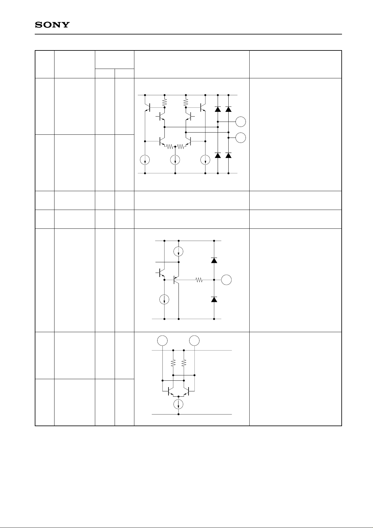
Pin Description
CXA3003R
Pin
No.
1
2
3
4
5
Symbol
GND
RXVCO TI
RXVCO T2
GND RXIF
VDD RXIF
Typical
Voltage (V)
DC AC
0 V
0 V
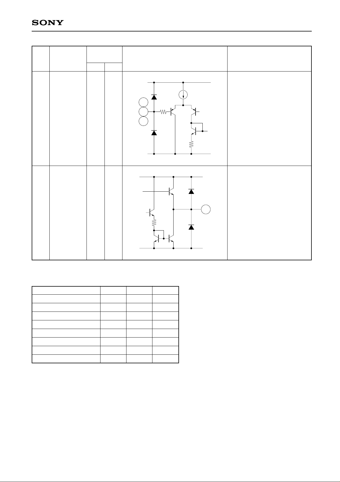
3.3 V
Equivalent circuit
2 3
1k 1k
Description
Negative power supply pin.
VDD RXIF
Receive VCO tuning pins.
Connected to an external LC
tank circuit for setting the
receive VCO frequency.
GND RXIF
Negative power supply pin for
RXIF block.
Positive power supply pin
for RXIF block.
VDD RXIF
6
7
8
RXIFB
RXIF
RSSI
2 V
2 V
2502k250
2k 2k
2k
GND RXIF
VDD RXIF
Analog differential receive IF
input pins.
Analog RSSI output pin.
6
7
150
8
9
10
GND RX
VDD RX
0 V
3.3 V
GND RXIF
Negative power supply pin for
RX block.
Positive power supply pin for
RX block.
—3—
CXA3003R
Pin
No.
11
12
13
14
Symbol
TXIFB
TXIF
GND TXIF
VDD TXIF
Typical
Voltage (V)
DC AC
2.1 V
2.1 V
0 V
3.3 V
Equivalent circuit
400
200
400
200
VDD TXF
VDD TXIF
GND TXIF
Description
11
Analog differential transmit IF
12
output pins.
Negative power supply pin for
TXIF block.
Positive power supply pin for
TXIF block.
15
16
17
FM MOD
TVCO T1
TVCO T2
1.5 V
16 17
1k 1k
150
GND TXF
15
VDD TXIF
GND TXIF
Analog baseband signal output
pin for FM.
Transmit VCO tuning pins.
Connected to an external LC
tank circuit for setting the
transmit VCO frequency.
—4—

CXA3003R
Pin
No.
18
19
Symbol
PD ISET
PD OUT
Typical
Voltage (V)
DC AC
0.64 V
Equivalent circuit
VDD TXF
150
GND TXF
VDD TXF
6.25k
150
19
18
Description
Current of PD OUT setting pin.
Transmit synthesizer charge
pump output pin.
20
GND SYNTH
21
VDD SYNTH
22
23
24
GND TXF
VDD TXF
LOCK DET
0 V
3.3 V
0 V
3.3 V
6.25k
VDD SYNTH
150
GND TXF
24
Negative power supply pin for
PLL block.
Positive power supply pin for
PLL block.
Negative power supply pin for
TX block.
Positive power supply pin for
TX block.
Transmit IF synthesizer lock
detect output pin.
GND SYNTH
—5—
CXA3003R
Pin
No.
26
39
25
27
28
30
35
36
Symbol
TCXO
GND ESD
NC
Typical
Voltage (V)
DC AC
2.2 V
0 V
Equivalent circuit
150
26
20k 20k
Description
VDD SYNTH
Input pins for External clock
19.68 MHz (TCXO).
GND SYNTH
Negative power supply pin.
Don't connect pins.
29
31
32
TCXO4
CAP1
CAP2
VDD DAC
150
GND ESD
VDD RX
31
32
29
Output pin for TCXO/4
frequency.
The pins for External
Capacitor.
33
34
37
DNC
GND DAC
0 V
GND RX
Don't connect any line to this
pin.
Negative power supply pin for
TXDA block.
—6—

CXA3003R
Pin
No.
38
40
to
47
48
49
50
51
Symbol
VDD DAC
TXD0
to
TXD7
TXCLK,
TXCLKB
GND BUF
VDD BUF
Typical
Voltage (V)
DC AC
3.3 V
0 V
3.3 V
Equivalent circuit
40
45
41
46
42
47
43
48
44
49
60k
Description
Positive power supply pin for
TXDA block.
VDD DAC
Transmit Data input pins for
Transmit 8 bit D/A converter.
TXD7 is the MSB.
Differential transmit Clock input
pins for Transmit 8 bit D/A
converter.
GND DAC
Negative power supply pin for
A/D output block.
Positive power supply pin for
A/D output block.
52
53
to
56
57
to
60
61
CHIP x 8
RXID0
to
RXID3
RXQD0
to
RXQD3
RXFMSTRB
61
62
100k
VDD BUF
GND BUF
VDD ADC
52
53
54
55
56
57
58
59
60
Output pin for CHIPx8 divider
with a ratio of
512/1025xTCXO.
Output pins for Receive
CDMA 4 bit A/D converter of I
signal. RXID3 is the MSB.
Output pins for Receive
CDMA 4 bit A/D converter of Q
signal. RXQD3 is the MSB.
Strobe input pin for Receive
FM 8 bit A/D converter.
62
FMCLK
Clock input pin for Receive FM
8 bit A/D converter.
GND ADC
—7—
CXA3003R
Pin
No.
63
64
65
66
67
68
Symbol
RXQFMDT
RXIFMDT
DNC
GND ADC
VDD ADC
Typical
Voltage (V)
DC AC
0 V
3.3 V
Equivalent circuit
VDD BUF
GND BUF
Description
Q serial data output pin for
Receive FM 8bit A/D converter.
63
64
I serial data output pin for
Receive FM 8bit A/D converter.
Don't connect any line to this
pins.
Negative power supply pin for
A/D converter block.
Positive power supply pin for
A/D converter block.
69
70
71
72
QOFFSET
IOFFSET
HKADVCC
NC
1.5 V
1.5 V
3.3 V
22k
100k
30k
142k
30k
142k
150
150
VDD RX
GND RX
69
70
Receive Q channel offset
adjust input pin.
Receive I channel offset adjust
input pin.
Positive power supply pin for
HKA/D converter block.
Don't connect pin.
—8—
CXA3003R
Pin
No.
73
74
75
Symbol
ADCCLK
ADCDT
ADCENBL
Typical
Voltage (V)
DC AC
Equivalent circuit
60k
75
Description
VDD BUF
Clock output pin for House
Keeping 8 bit A/D converter.
73
74
Serial data output pin for
House Keeping 8 bit A/D
converter.
GND BUF
VDD BUF
Enable input pin for House
Keeping 8 bit A/D converter.
76
ADCIN
1.5 V
GND BUF
HKADVCC
A/D analog input pin for House
Keeping 8 bit A/D converter.
76
48.5k
GND ADC
—9—
CXA3003R
Pin
No.
77
78
79
80
Symbol
SLEEPB,
IDLEB,
FMB
RXVCOOUT
Typical
Voltage (V)
DC AC
0 V
Equivalent circuit
77
78
79
150
VDD ADC
GND ADC
VDD RXIF
80
Description
Test mode switch pins.
These pins control this IC
function mode (∗1).
Receive VCO output pin
connected the external PLL IC.
∗
1 Function Mode
Function Mode
CDMA RXTX
CDMA Idle
CDMA Sleep
FM RXTX
FM Idle
FM Idle (Transition)
FM RXTX (Transition)
CDMA Sleep (Transition)
FMB
high
high
high
low
low
low
low
high
IDLEB
high
low
low
high
low
low
high
high
SLEEPB
high
high
low
high
high
low
low
low
GND RXIF
Mode functions explain:
1. CDMA RXTX :
This mode requires everything except the FMspecific circuits to be operating.
2. CDMA Idle :
This mode powers down all transmit circuits
and FM receive.
3. CDMA Sleep :
This mode powers down everything except
the TCXO divider and TCXO/4 output driver.
4. FM RXTX :
This mode powers down all CDMA-specific
circuits except the CHIPx8 synthesizer.
5. FM Idle :
This mode powers down all transmit and
CDMA Receive circuits.
—10—
 Loading...