

Sony CXA3001N Datasheet

CXA3001N
For the availability of this product, please contact the sales office.
RX Gain Control Amplifier
Description
CXA3001N is an RX gain control amplifier for
CDMA cellular mobile phone.
Features
• Wide gain control range
• Linear gain slope
• Noise figure Typ. 6dB at Gain = 45dB
• Output IP3 Typ. +2dBm at Gain = 40dB
• 2 input ports
• Power save function included
Absolute Maximum Ratings
• Supply voltage VCC 6V
•Operating temperature Topr –40 to +85 °C
• Storage temperature Tstg –65 to +150 °C
• Allowable power dissipation PD 420 mW
• Supply voltage range –0.3 to 6 V
• Logic input voltage –0.3 to VCC +0.3 V
• Signal input voltage –0.3 to VCC +0.3 V
• Differential signal input voltage 0 to 2.5 V
24 pin SSOP (Plastic)
Operating Conditions
Supply voltage 3.1 to 3.8 V
Applications
• CDMA cellular mobile phone
• CDMA & AMPS cellular phone
Structure
Bipolar sillicon monolithic IC
Sony reserves the right to change products and specifications without prior notice. This information does not convey any license by
any implication or otherwise under any patents or other right. Application circuits shown, if any, are typical examples illustrating the
operation of the devices. Sony cannot assume responsibility for any problems arising out of the use of these circuits.
– 1 –
E95711-PP
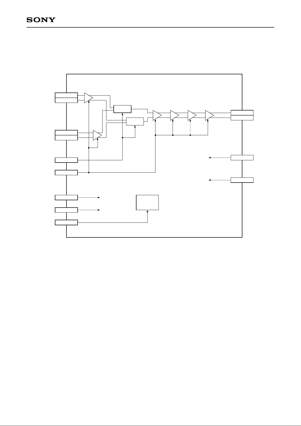
Block Diagram
CXA3001N
IF Input
for CDMA
IF Input
for FM
Input Select
Gain Control
Supply Voltage
Ground
Power Save
CDMAIN
CDMAINX
FMIN
FMINX
MODE
GCTL
VCC1, 2
GND1, 2
PSV
SWITCH
SWITCH
Bias
Driver
CXA3001N
OUT
OUTX
BP1
BP2
IF Output
to External
Capacitor
– 2 –
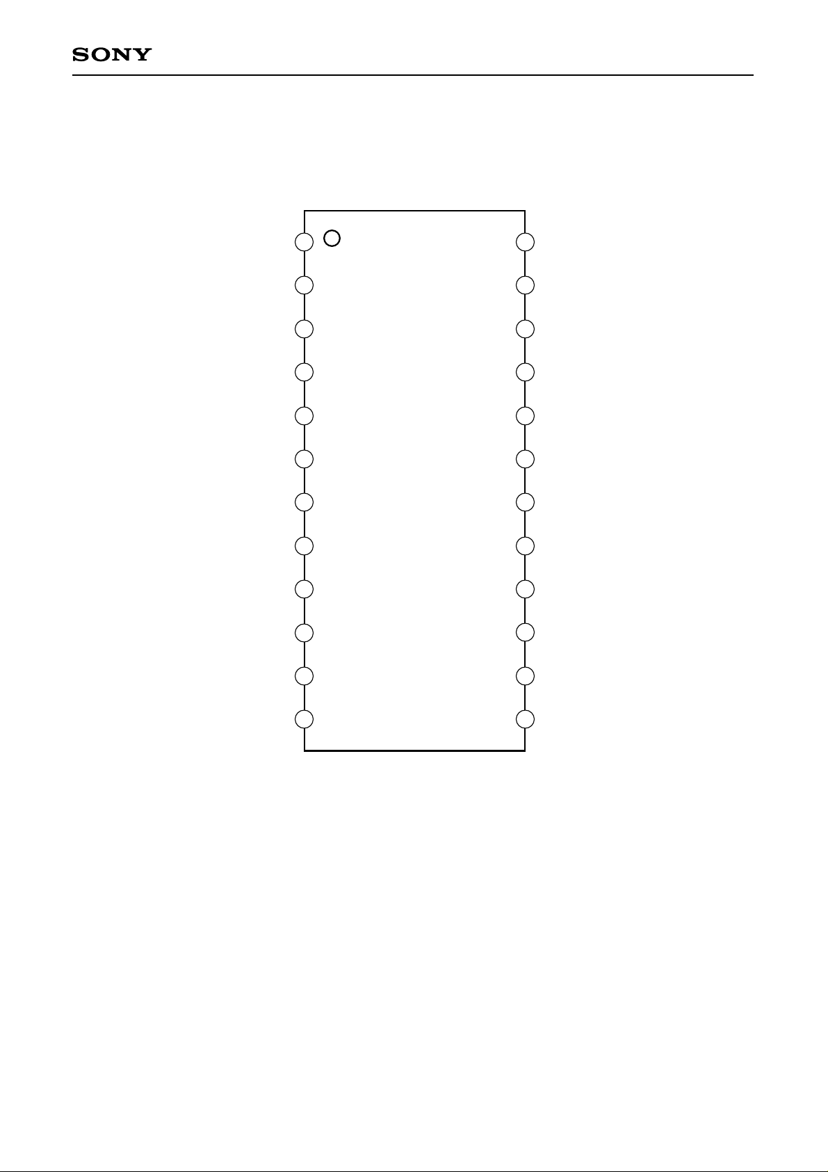
Pin Configuration
CXA3001N
CC1
V
GND1
NC
NC
NC
FMIN
NC
1
2
3
4
5
6
CXA3001N
7
8
9
10
MODE PSV
CDMAIN
CDMAINX
23
22
20
19
18
17
16
15
24
21
GCTL
NC
NC
NC
OUTX
NC
OUT
NC
CC2
V
11
FMINX
12
BP1 BP2
14
13
GND2
– 3 –
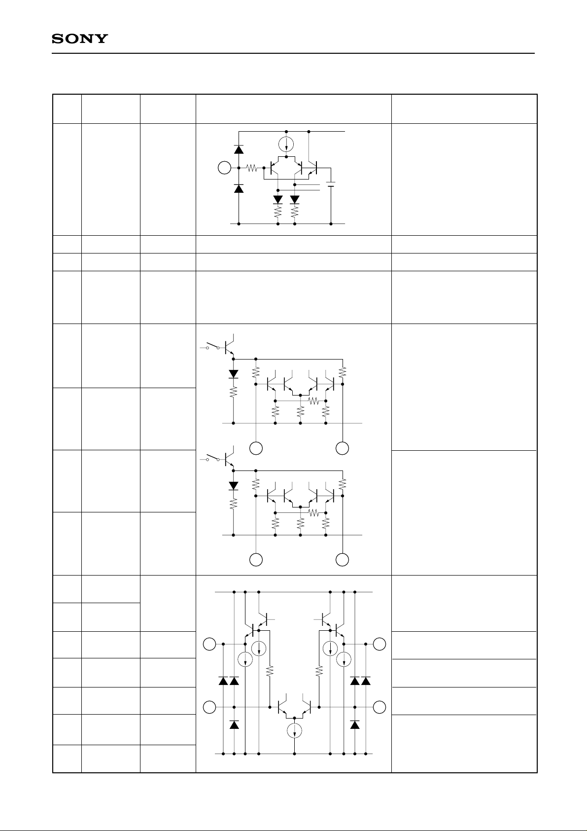
Pin Description
CXA3001N
Pin
No.
Symbol
1 MODE
Pin voltage
Typ. (V)
Equivalent circuit Description
VCC1
30k
1
Input select pin.
CDMAIN for High.
FMIN for Low.
GND1
2VCC1 3.6 Positive power supply.
3 GND1 0 Ground.
4
6
N.C.
8
No connection.
10
5 CDMAIN
1.2
2k2k
Differential input pins for
received CDMA IF signal.
7 CDMAINX 1.2
9
FMIN
11 FMINX
1.2
1.2
12 BP1
2.4
13 BP2
14
GND2 0
15 VCC2
3.6
16 N.C.
19
12
GND1
5
7
2k2k
Differential input pins for
received FM IF signal.
GND1
9
11
VCC2
Connected to GND with
capacitor 0.01µF.
17
Ground for output stage.
20k
20k
Positive power supply for
output stage.
No connection.
13
17 OUT 1.7
19 OUTX 1.7
Differential output pins for
received IF signal.
GND2
– 4 –
 Loading...