

Sony CXA2610AN Datasheet

Laser Driver
Description
The CXA2610AN is a laser driver IC for optical
discs. This IC supports higher optical power output
speeds.
Features
• LD driver with excellent driving capability
• Write current of 250mA (max.) possible by setting
the IIN2 (Pin 2) and IIN3 (Pin 5) external resistors
• Rise time ≈ 3ns
• Fall time ≈ 4ns
• The oscillation frequency of the built-in oscillation
circuit can be set from 100 to 600MHz by
connecting the OSCFR (Pin 4) external resistor to
GND.
• The oscillator amplitude initial value of the built-in
oscillation circuit can be set by connecting the
OSCGA (Pin 12) external resistor to GND, and the
oscillator amplitude can be adjusted by the IINR
input current value.
• Oscillation ON/OFF can be set as desired.
• Single +5V power supply
• TTL/CMOS control for control system
Applications
• CD-R driver
• CD-RW driver
• DVD driver
• Writable optical driver
• Laser diode current switching
Structure
Bipolar silicon monolithic IC
Absolute Maximum Ratings
• Supply voltage Vcc 5.5 V
• Operating temperature Topr –10 to +70 °C
• Storage temperature Tstg –65 to +150 °C
Operating Conditions
Supply voltage 4.5 to 5.5 V
– 1 –
PE00145-PS
Sony reserves the right to change products and specifications without prior notice. This information does not convey any license by
any implication or otherwise under any patents or other right. Application circuits shown, if any, are typical examples illustrating the
operation of the devices. Sony cannot assume responsibility for any problems arising out of the use of these circuits.
CXA2610AN
16 pin SSOP (Plastic)
Preliminary
– 2 –
CXA2610AN
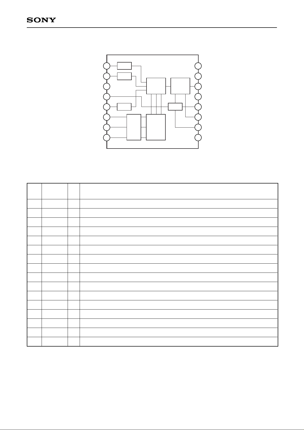
Pin Description
Pin
No.
1
2
3
4
5
6
7
8
9
10
11
12
13
14
15
16
Symbol
IINR
IIN2
GND
OSCFR
IIN3
CONTR
CONT2
CONT3
Vcc
OSCENA
ENABLE
OSCGA
GND
LD0
Vcc
Vcc
I/O
I
I
—
I
I
I
I
I
—
I
I
I
—
O
—
—
Description
Oscillation level adjustment.
LD drive current setting input.
Ground.
Oscillation frequency adjustment.
LD drive current setting input.
LD drive current output setting.
LD drive current output setting.
LD drive current output setting.
VCC.
Oscillation ON for read/forced oscillation ON control.
LD drive current ON/OFF control. (High: ON, Low: OFF)
Oscillation level initial value setting.
Ground.
LD anode side connection.
VCC.
VCC.
V-I
V-I
V-I
TTL
1
2
3
4
5
6
7
8
9
10
11
12
13
14
15
16
OSC
Driver
Current
SW
Delay
Vcc
Vcc
LD0
GND
OSCGA
ENABLE
OSCENA
Vcc
IINR
IIN2
GND
OSCFR
IIN3
CONTR
CONT2
CONT3
Block Diagram

– 3 –
CXA2610AN
OSC: L (write mode). LD: OFF
Current consumption for IINR input voltage where oscillation level =
47mAp-p
Current consumption when CONTR = Low for I
CC2 (OSC: ON)
Pin voltage measurement
Pin voltage measurement
Output current for IINR pin input 5V
Output current for IIN2 pin input 5V
Output current for IIN3 pin input 5V
Current gain measurement for IINR (∆I
OUT/∆IIN)
Current gain measurement for IIN2 (∆I
OUT/∆IIN)
Current gain measurement for IIN3 (∆I
OUT/∆IIN)
IOUT = 40mA (CONTR) + 40mA (CONT2), settling 10 to 90%
I
OUT = 40mA (CONTR) + 40mA (CONT2), settling 10 to 90%
I
OUT = 40mA (CONTR) + 40mA (CONT2)
Time from 50% of CONT3 (High
→ Low) to 50% of output final value
Time from 50% of CONT3 (Low → High) to 50% of output final value
Time from 50% of ENABLE (Low → High) to 50% of output final value
Time from 50% of ENABLE (High → Low) to 50% of output final value
Oscillation frequency
Oscillation level when IINR = 2V
CONTR, CONT2, CONT3, OSCENA, ENABLE
CONTR, CONT2, CONT3, OSCENA, ENABLE
Input impedance for IINR, IIN2 and IIN3
1.21
80
115
145
14595120
120
60
2
175
40
60
83
1.257
103
125
157
163
104
133
136
3
4
—
3.1
3.4
4.4
2.2
189
77
252
1.3
120
145
175
175
115
145
145
85
1.3
375
mA
mA
mA
V
mV
mA
mA
mA
—
—
—
ns
ns
%
ns
ns
ns
ns
MHz
mAp-p
V
V
Ω
1
2
3
4
5
6
7
8
9
10
11
12
13
14
15
16
17
18
19
20
21
22
23
Current consumption 1
Current consumption 2
Current consumption 3
Pin voltage 1
Pin voltage 2
Output drive current
Output drive current
Output drive current
Input/output current gain
Input/output current gain
Input/output current gain
Rise time
Fall time
Overshoot
CONT delay 1
CONT delay 2
LD delay 1
LD delay 2
Oscillation frequency
Oscillation level
Logic Low level
Logic High level
Input resistance
I
CC1
ICC2
ICC3
VFR
VLE
I
OUT1IOUT2IOUT3IGAIN1IGAIN2IGAIN3
TR
TF
OVS
CDELAY1
CDELAY2
LDELAY1
LDELAY2
OSCFR
OSCLE
VTHL
VTHH
ZIN
2.0
1.3
—
—
1.3
2.0
1.3
2.0
1.3
2.0
1.3
1.3
—
—
—
2.0
—
—
2.0
1.3
2.0
2.0
1.3
2.0
H → L
L → H
H → L
1.3
2.0
2.0
—
—
—
2.0
—
—
2.0
1.3
2.0
1.3
2.0
H → L
H → L
2.0
—
—
—
1.3
2.0
1.3
2.0
1.3
2.0
2.0
1.3
2.0
—
—
—
1.3
2.0
2.0
2.0
L → H
H → L
2.0
—
—
—
Measure-
ment No.
Measurement item Symbol
CONTR CONT2 CONT3
OSCENA
ENABLE
Control status
Measurement condition and method Min. Typ. Max. Unit
Electrical Characteristics (Ta = 25°C, Vcc = 5V)
AC items
Logic
 Loading...