

Sony CXA2586M Datasheet
—1—
E99430B01
Sony reserves the right to change products and specifications without prior notice. This information does not convey any license by
any implication or otherwise under any patents or other right. Application circuits shown, if any, are typical examples illustrating the
operation of the devices. Sony cannot assume responsibility for any problems arising out of the use of these circuits.
Absolute Maximum Ratings (Ta=25 °C)
• Supply voltage VCC 5.5 V
• Operating temperature Topr –10 to +70 °C
• Storage temperature Tstg –40 to +100 °C
• Allowable power dissipation
PD 300 mW
Operating Conditions
• Supply voltage1 VCC 4.5 to 5.5 V
• Supply voltage2 VC 1.5 to VCC–1.5 V
Structure
Bipolar silicon monolithic IC
Description
CXA2586M is a PDIC (photodetector IC)
developed as a photodetector for the optical pickup
of CD-ROM/DVD-ROM.
The photodiode and circuit blocks operate at high
speed. (Typ. 100MHz)
• Focus servo : astigmatic method
• Tracking servo (CD)
: three-spot method
• Tracking servo (DVD)
: differential phase detection method
Features
• High-speed I-V amplifier
(current-voltage conversion circuit)
• High-speed photodiode
• Adding amplifier (addition of A to D)
• Compact transparent molded package (SOP)
Applications
Optical pickup for CD-ROM/DVD-ROM
PDIC for CD-ROM/DVD-ROM
PD-S-19-B (Plastic)
CXA2586M
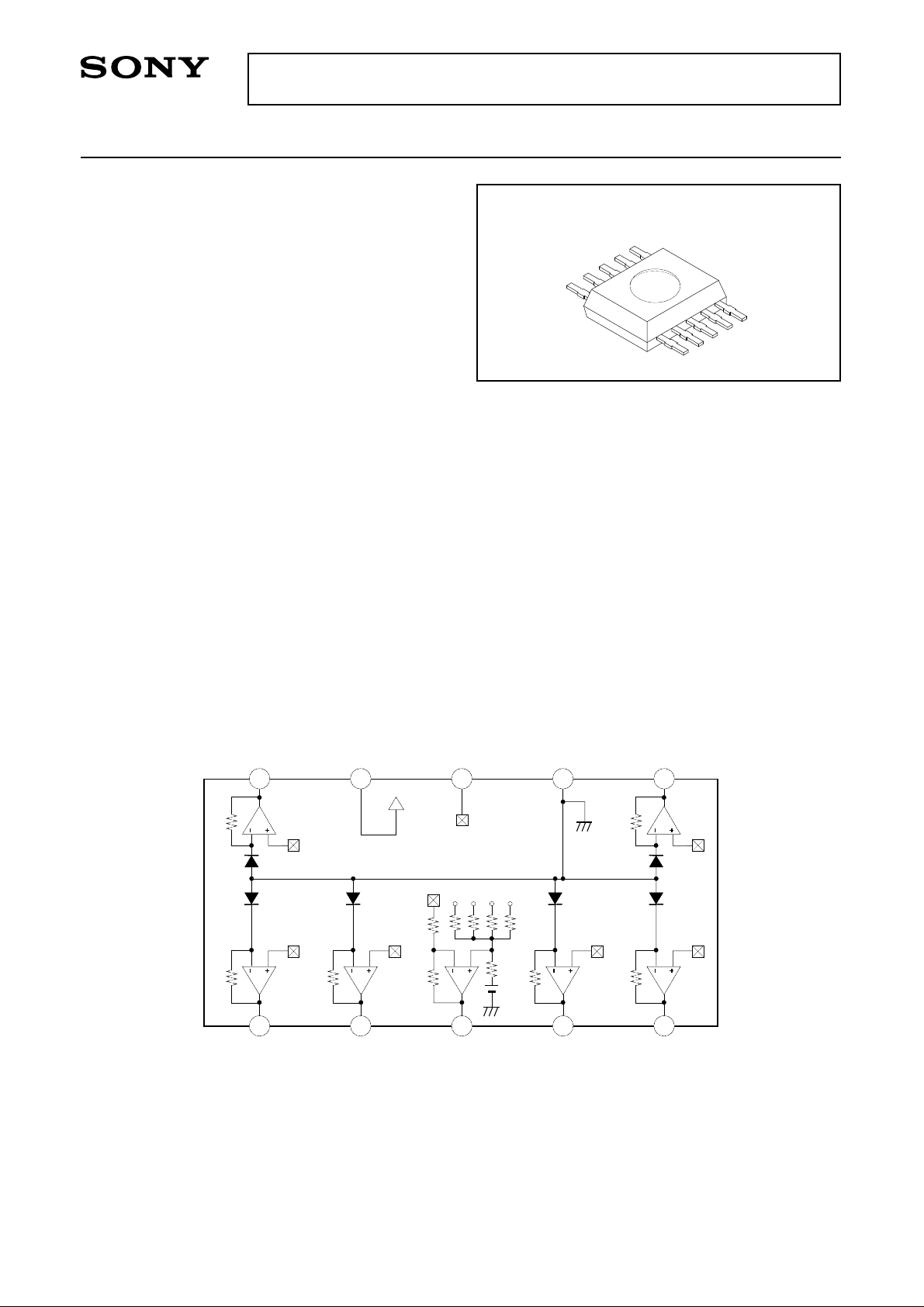
Block Diagram and Pin Configuration
1 2 3 4 5
689
10
7
Fo VCC VC GND
VREF
Eo
Do Ao
Ao Bo Co Do
RF Bo Co
∗ The components marked by A, B, C, D, E and F are the photodiodes
(photo sensitivity. About 0.4A/W @650nm, 780nm)

—2—
CXA2586M
Pin Description
Pin No.
2
4
1
5
6
10
3
7
8
9
Symbol
Ao
Bo
Co
Do
Eo
Fo
RF
GND
Vc
VCC
I/O
O
O
O
I
I
I
1
2
4
5
6
10
300
200µA
37k
37k
V
C
3
7k
8
Description
Output of voltage signals converted
from optical signals
Output of voltage signals converted
from optical signals
Output of addition of Ao to Do
For dual power supply
: negative power supply
For a single power supply
: GND
For dual power supply
: GND
For a single power supply
: center voltage input
Positive power supply
Equivalent circuit
—3—
CXA2586M
Electrical and Optical Characteristics (VCC=5.0 V, VC=2.5 V, Ta=25 °C)
Item
Current consumption
Output offset voltage (A to D)
Output offset voltage (E, F)
Output offset voltage (RF)
Output voltage difference
Sum of output offset voltages
Output voltage (A to D)
Output voltage (E, F)
Output voltage (RF)
Output voltage ratio (E, F/A to D)
Output voltage ratio (RF/A to D)
Maximum output voltage (A to D)
Maximum output voltage (E, F)
Maximum output voltage (RF)
Frequency response (A to D)
Frequency response (E, F)
Frequency response (RF)
Group delay difference (A to D)
Group delay difference (RF)
Output noise level (A to D)
Output noise level (RF)
Symbol
ICC
Voff
Voff
Voff
∆Voff
Voffs
Vo
Vo
Vo
VOR
VOR
Vo
Vo
Vo
fc
fc
fc
∆ Gd
∆ Gd
Vn
Vn
Conditions
In the dark
In the dark, Vc reference
In the dark, Vc reference
In the dark, GND reference
A-B, in the dark
C-D, in the dark
(A+C) – (B+D), in the dark
E-F, in the dark
A+B+C+D, in the dark
λ=650 nm, 780 nm, Po=10 µW
λ=650 nm, 780 nm, Po=10 µW
λ=650 nm, 780 nm, Po=10 µW
λ=650 nm, 780 nm, Po=10 µW
λ=650 nm, 780 nm, Po=10 µW
λ=650 nm, 780 nm, Po=100 µW
λ=650 nm, 780 nm, Po=100 µW
λ=650 nm, 780 nm, Po=100 µW
λ=650 nm, 780 nm
Po=10 µWDC, 4 µWp-p
100 kHz reference, –3 dB
λ=650 nm,780 nm
Po=10 µWDC, 4 µWp-p
100 kHz reference, –3 dB
λ=650 nm, 780 nm
Po=10 µWDC, 4 µWp-p
100 kHz reference, –3 dB
100 kHz to 50 MHz
100 kHz to 50 MHz
f=50 MHz, RBW=30 kHz
f=50 MHz, RBW=30 kHz
Min. Typ. Max. Unit
— 15 20 mA
–25 0 25 mV
–15 0 15 mV
1.25 1.4 1.55 V
–20 0 20 mV
–20 0 20 mV
–20 0 20 mV
–15 0 15 mV
–100 0 100 mV
180 246 312 mV
312 447 581 mV
302 432 561 mV
1.71 1.81 1.90 —
1.67 1.76 1.84 —
3.8 4.0 — V
3.8 4.0 — V
3.8 4.0 — V
70 100 — MHz
15— MHz
80 105 — MHz
— 15ns
— 15ns
—–87 –82 dBm
—–76 –71 dBm
Note 1) Output offset voltage: Vc is the reference for A to F, GND for RF.
Note 2) Output voltage: Vc is the reference for A to F, GND for RF. However, the offset voltage is excluded.
Note 3) Output voltage, frequency response, group delay, output noise level: Confirmation of design.
Note 4) Measurement by the optical input: Measurement is made by emitting the light to the center of each
photodiode.
In regard of the frequency response of A to D and RF, the same response can be obtained by emitting
the light to the A to D photodiodes evenly.
 Loading...