

Sony CXA2581N Datasheet
RF Signal Processor for CD Players
Description
The CXA2581N is an RF signal processing IC for
compact disc players.
Features
• Wide band RF signal processing
• RF system VCA circuit
• RF system equalizer (supports CAV mode)
• Supports pickups with built-in RF summing
amplifier
• Low current consumption mode (EQ Pass mode)
• RW/ROM switching mode
• Center error amplifier
• Output DC level shift circuit
• TE balance adjustment function
Functions
• RF AC summing amplifier, equalizer, VCA
• RF DC summing amplifier
• Focus error amplifier
• Tracking error amplifier
• Center error amplifier
• Automatic power control
• VC buffer amplifier (analog block, digital block)
Absolute Maximum Ratings
• Supply voltage VCC 7V
• Storage temperature Tstg –65 to +150 °C
• Allowable power dissipation
PD 620 mW
Operating Conditions
• Operating supply voltage range
VCC – GND 3.4 to 5.5 V
(0V ≤ Vcc – DVcc < 2V)
Note) Care should be taken for the operating voltage.
See page 18.
• Operating temperature Topr –30 to +85 °C
– 1 –
E98739A97-PS
Sony reserves the right to change products and specifications without prior notice. This information does not convey any license by
any implication or otherwise under any patents or other right. Application circuits shown, if any, are typical examples illustrating the
operation of the devices. Sony cannot assume responsibility for any problems arising out of the use of these circuits.
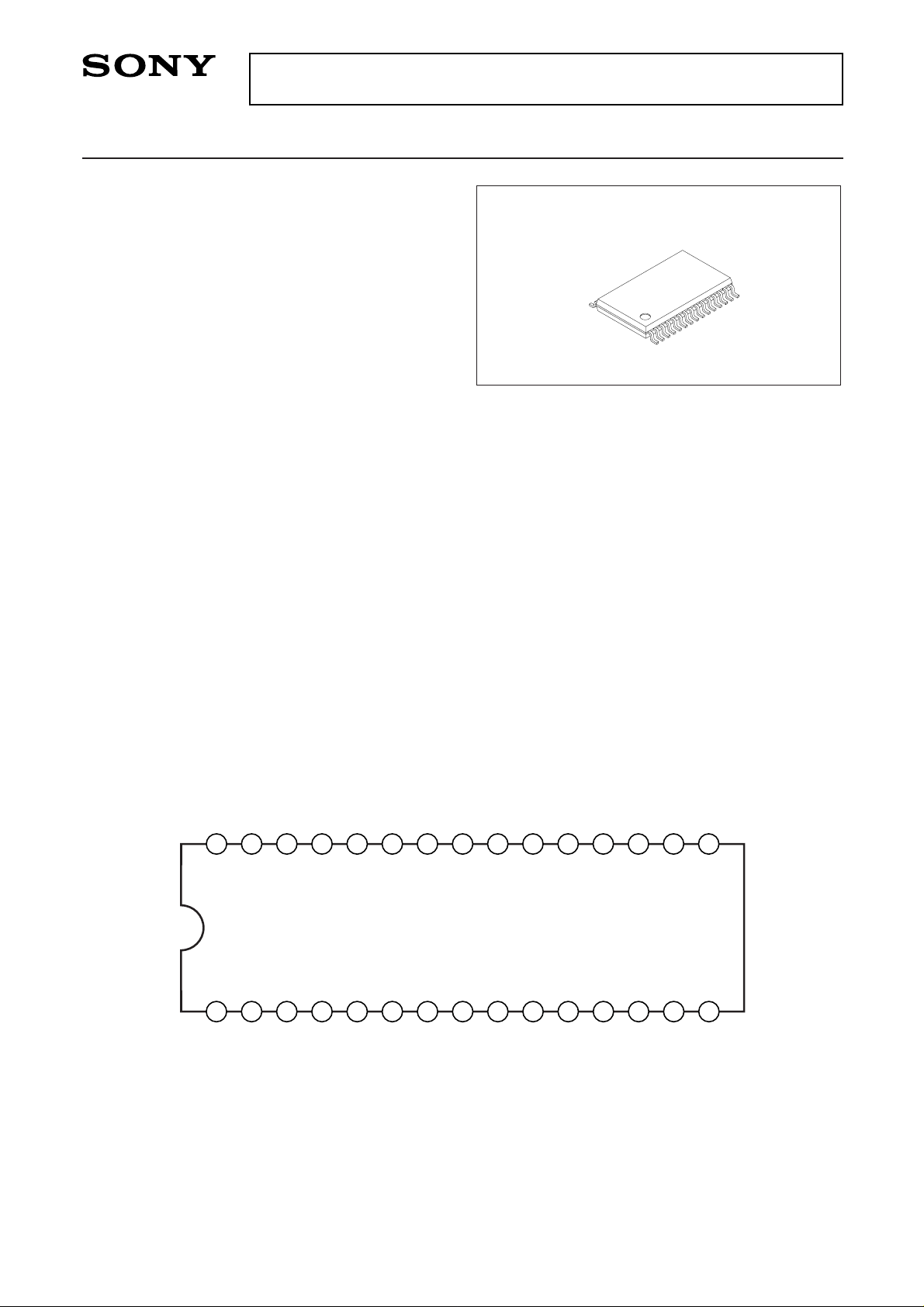
CXA2581N
30 pin SSOP (Plastic)
Pin Configuration
1 2 3 4 5 6 7 9 1211
20 192224252627282930
8 10 1413
18 172123
15
16
LD
PD
EQ_IN
AC_SUM
GND
A
B
D
SW
F
C
E
DVC
DV
CC
RFAC
DC_OFST
RFDCI
RFDCOVCRFC
VFC
BST
V
CC
TE_BAL
CE
RFG
CEI
FEITEFE
– 2 –
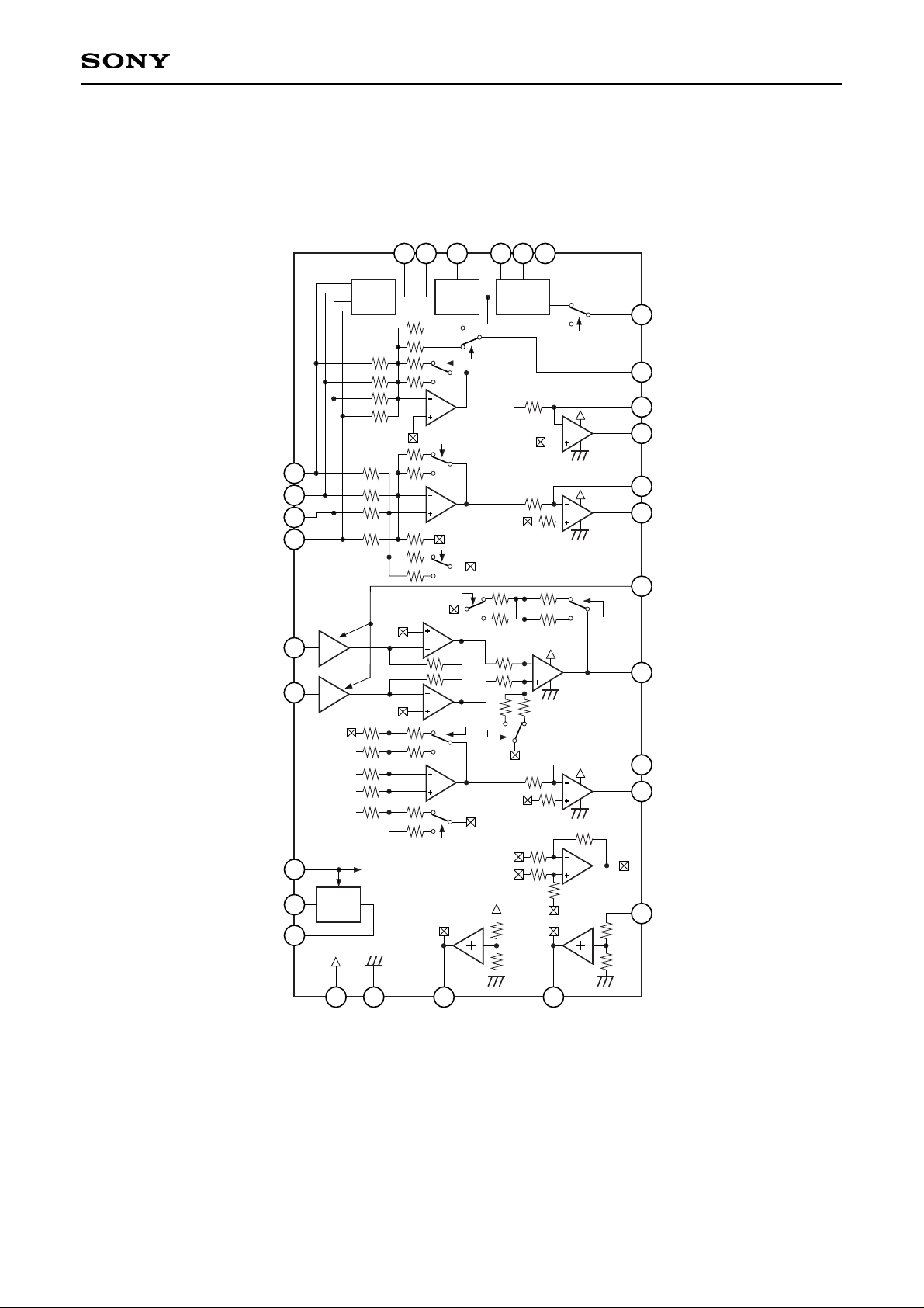
CXA2581N
Block Diagram
DVCC
AC
SUM
APC
AC
VCA
EQ
VC
VC
VC
RW/ROM
EQ_ON/OFF
VOFST
DVC
DV
CC
RW/ROM
VC
RW/ROM
RW/ROM
RW/ROM
DVC
DV
CC
25
15
30
29
28
17
16
26242334
6
7
8
9
10
19
18
DVC
DV
CC
DVC
VC
VC
VOFST
DVC
DVC
V
CC
VOFST
B
C
A
D
A
B
C
D
F
E
SW
PD
LD
VCC
GND
VC
DVC
DVCC
CE
CEI
TE
TE_BAL
FE
FEI
RFDCO
RFDCI
RFAC
VFC
RFC
RFG
BST
EQ_IN
AC_SUM
DC_OFST
VC
RW/ROM
21
145
20
13
VC
VCC
APC-OFF (Hi-Z)
RW/ROM
(H/L)
2722
1
2
12
11
gm
gm
RW/ROM
VOFST
– 3 –
CXA2581N
Pin Description
Pin
No.
1
2
3
4
5
6
7
8
9
10
11
12
13
14
15
16
17
18
19
20
21
22
23
24
25
26
27
28
29
30
LD
PD
EQ_IN
AC_SUM
GND
A
B
C
D
E
F
SW
DVCC
DVC
RFAC
FE
FEI
TE
TE_BAL
CE
CEI
VCC
RFG
BST
VFC
RFC
VC
RFDCO
RFDCI
DC_OFST
APC amplifier output.
APC amplifier input.
RFAC system VCA block and EQ block input.
RFAC system RF SUM output.
GND.
A signal input.
B signal input.
C signal input.
D signal input.
E signal input.
F signal input.
Mode switching signal input.
DVCC.
DVC output.
RFAC signal output.
Focus error signal output.
FE amplifier virtual ground.
Tracking error signal output.
TE balance adjustment.
Center error signal output.
CE amplifier virtual ground.
VCC.
RFAC system VCA block low frequency gain adjustment.
EQ boost level adjustment.
EQ cut-off frequency adjustment.
EQ cut-off frequency adjustment.
VC voltage output.
RFDC signal output.
RFDC amplifier virtual ground.
RFDC signal output offset adjustment.
O
I
I
O
I
I
I
I
I
I
I
I
I
O
O
O
I
O
I
O
I
I
I
I
I
I
O
O
I
I
Symbol I/O Description
– 4 –
CXA2581N
Pin Description
Pin
No.
Symbol I/O Equivalent circuit Description
1
10k
1k
2
55k
20k
20k
3
1.2k
1.1k
VC
1.1k
5k
5k
VC
1.6k1.6k
4
1
2
3
4
O
I
I
O
LD
PD
EQ_IN
AC_SUM
5 GND
APC amplifier output.
APC amplifier input.
Equalizer circuit input.
RFAC summing amplifier
output.
— —
GND.
– 5 –
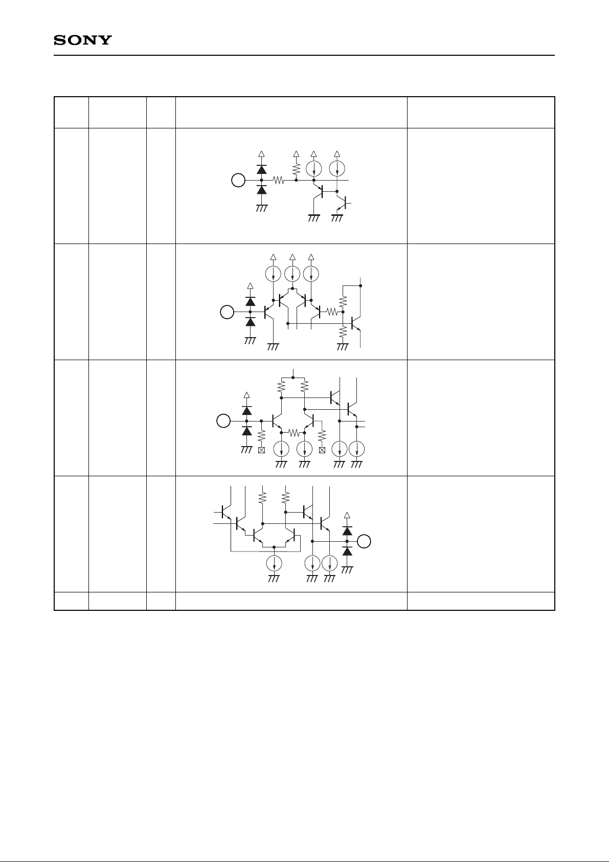
CXA2581N
Pin
No.
Symbol I/O Equivalent circuit Description
47k
VC
47k
15k
30k
100µA
100µA
100µA
6
100µA
7
8
9
10
11
VC
200k
200k
200k
12
VC
14
150k
150k
25
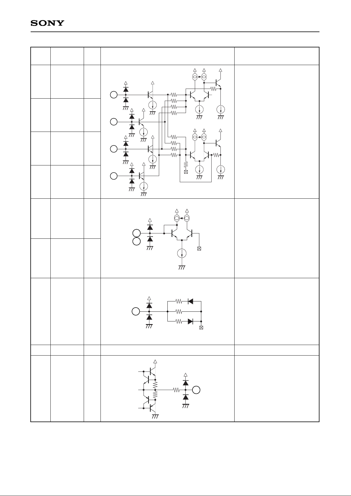
6 IA
7 IB
8 IC
9 ID
RF summing amplifier and
focus error amplifier input.
10IE
Tracking error amplifier input.
11
I
F
12 ISW
CD-ROM/RW switching input.
RW when connected to VCC,
ROM when connected to GND.
14 ODVC
(DVCC + GND)/2 voltage
output.
13
— —
DVCC
Digital power supply.
– 6 –
CXA2581N
Pin
No.
Symbol I/O Equivalent circuit Description
15
100
2mA
15 ORFAC RFAC amplifier output.
17 IFEI
Focus error amplifier gain
adjustment. The gain is
adjusted by the external
resistance value connected
between this pin and Pin 16.
50k
124
VC
16
124
17
16 OFE Focus error amplifier output.
19ITE_BAL
Tracking error E and F gain
balance adjustment.
20k
18
19
20k
20k
VC
18 OTE
Tracking error amplifier output.
21 ICEI
Center error amplifier gain
adjustment.
The gain is adjusted by the
external resistance value
connected between this pin
and Pin 20.
50k
124
VC
20
124
21
20 OCE Center error amplifier output.
– 7 –
CXA2581N
22 — —
VCC VCC. (AVCC)
Pin
No.
Symbol I/O Equivalent circuit Description
20k
VC
23
100µA
50µA
20k
VC
24
20k
VC
25
100µA
124
1.0V
26
27
150k
150k
25
23 I
RFG
Sets the RFAC low frequency
gain.
24 I
BST
Input for adjusting the
equalizer circuit boost level.
25 I
VFC
Input for adjusting the
equalizer circuit boost
frequency with the control
voltage.
26 I
RFC
Input for adjusting the
equalizer circuit boost
frequency with external
resistance.
27
O
VC
(VCC + GND)/2 voltage
output.
 Loading...