

Sony CXA2570N Datasheet

RF Matrix Amplifier
Description
The CXA2570N is an IC developed for the RF signal
processing of compact disc players.
Features
• Wide band RF signal processing
• RF system VCA circuit
• RF system equalizer (supports CAV mode)
• Supports pickups with built-in RF summing amplifier
• Low power consumption mode (EQ Pass mode)
• RW/ROM switching mode
Functions
• RFAC summing amplifier, equalizer, VCA
• RFDC summing amplifier
• Focus error amplifier
• Tracking error amplifier
• Automatic power control
• VC buffer amplifier
Applications
CD-ROM/RW compatible systems
Structure
Bipolar silicon monolithic IC
Absolute Maximum ratings
• Supply voltage Vcc 7 V
• Operating temperature Topr –20 to +75 °C
• Storage temperature Tstg –65 to +150 °C
• Allowable power dissipation
PD 620 mW
Operating Conditions
• Supply voltage Vcc – GND 3.0 to 5.5 V
• Operating temperature Topr –20 to +75 °C
– 1 –
E98259A98-PS
Sony reserves the right to change products and specifications without prior notice. This information does not convey any license by
any implication or otherwise under any patents or other right. Application circuits shown, if any, are typical examples illustrating the
operation of the devices. Sony cannot assume responsibility for any problems arising out of the use of these circuits.
CXA2570N
24 pin SSOP (Plastic)
– 2 –
CXA2570N
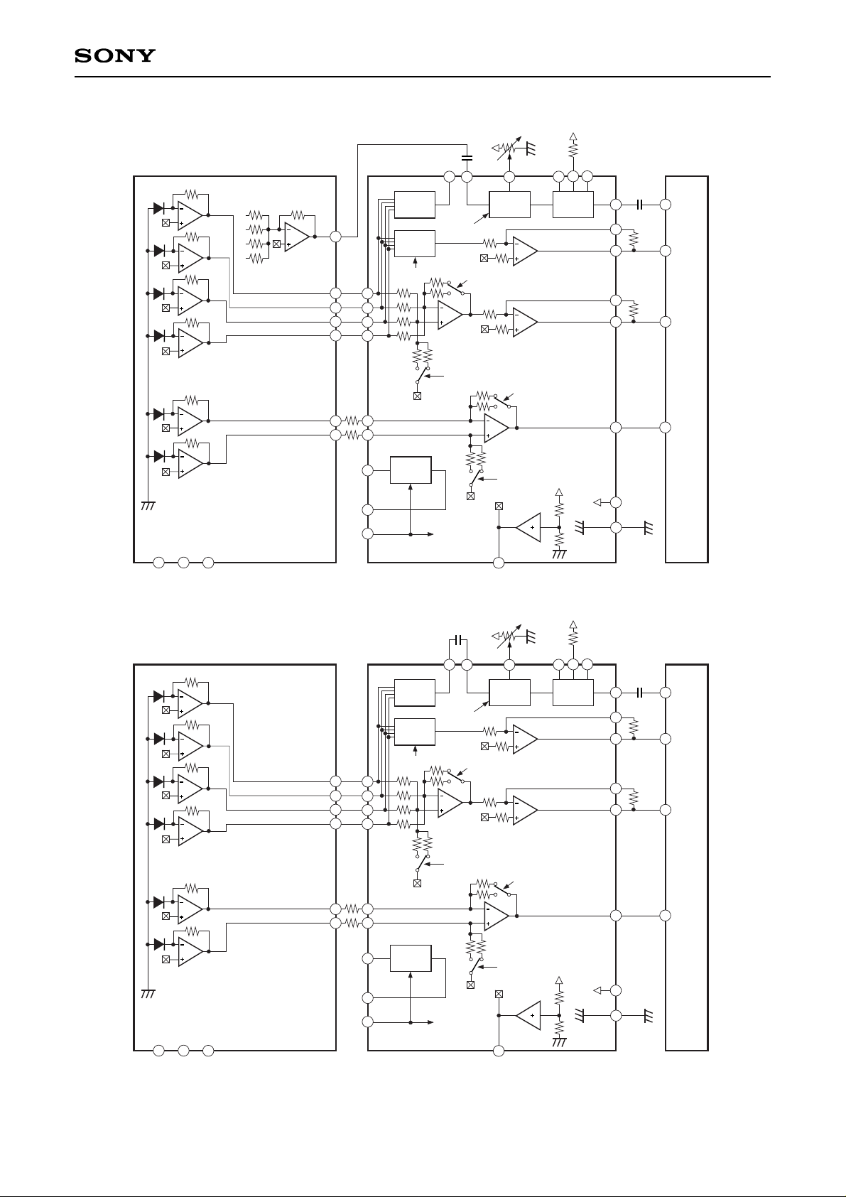
Connected Circuit Diagram
VC
RF
VC
A
A
B
C
D
A
B
C
D
A
B
C
D
AC
SUM
DC
SUM
VC
B
VC
VC
FE
FE
FEI
100k
VC
C
VC
D
VC
F F
E
F
E
VC
E
RFDCI
RFAC
RFAC
RFDCO
RFDC
5.1k
VC
ACG
RW/ROM RW/ROM
RW/ROM
RW/ROM
Rfc Vfc
5.1k
<DSP>
<OP (with RF_SUM)>
EQIACSUM BST
V
CC
VCC
VCC
TE
TE
GND
V
CC
0.1µ
AC
VCA
EQ
APC
VC
VC
RW/ROM
RW/ROM
PD
LD
SW
10k
10k
APC-OFF (Hi-Z)
RW/ROM
(H/L)
VCVCC GND
VCC
VCC
VCC
VC
A
A
B
C
D
A
B
C
D
AC
SUM
DC
SUM
VC
B
VC
VC
FE
FE
FEI
100k
VC
C
VC
D
VC
F F
E
F
E
VC
E
RFDCI
RFAC
RFAC
RFDCO
RFDC
5.1k
VC
ACG
RW/ROM RW/ROM
RW/ROM
RW/ROM
Rfc Vfc
5.1k
<DSP>
<OP (without RF_SUM)>
EQI
ACSUM
BST
V
CC
VCC
TE
TE
GND
0.1
AC
VCA
EQ
APC
VC
VC
RW/ROM
RW/ROM
PD
LD
SW
10k
10k
APC-OFF (Hi-Z)
RW/ROM
(H/L)
VC GNDVCC
VCC
– 3 –
CXA2570N
Pin Description
Pin
No.
1
2
3
4
5
6
7
8
9
10
11
12
13
14
15
16
17
18
19
20
21
22
23
24
LD
PD
EQ_IN
AC_SUM
GND
A
B
C
D
E
F
SW
RFAC
FE
FEI
TE
VCC
RFG
BST
VFC
RFC
VC
RFDCO
RFDCI
Out
In
In
Out
In
In
In
In
In
In
In
In
Out
Out
—
Out
In
In
In
In
In
Out
Out
—
APC amplifier output.
APC amplifier input.
RFAC system VCA block and EQ block input.
RFAC system RF SUM output.
Ground.
A signal input.
B signal input.
C signal input.
D signal input.
E signal input.
F signal input.
Mode switching signal input.
RFAC signal output.
Focus error signal output.
FE amplifier virtual ground.
Tracking error signal output.
VCC.
RFAC system VCA block low-frequency gain adjustment.
EQ boost amount adjustment range.
EQ cut-off frequency adjustment.
EQ cut-off frequency adjustment.
VC voltage output.
RFDC signal output.
RFDC amplifier virtual ground.
Symbol I/O Description

– 4 –
CXA2570N
Pin Description and Equivalent Circuit
Pin
No.
1
2
3
4
5
O
I
I
O
— —
APC amplifier output.
APC amplifier input.
Equalizer circuit input.
RFAC summing amplifier
output.
Ground.
LD
PD
EQ_IN
AC_SUM
GND
Symbol I/O Equivalent circuit Description
10k
1k
1
20k
55k
20k
2
VCVC
1.2k
5k5k
1.1k1.1k
3
1.6k
1.6k
4

– 5 –
CXA2570N
Pin
No.
6 I
RF summing amplifier and
focus error amplifier input.
A
7 IB
8 IC
9 ID
10 I
Tracking error amplifier input.
E
11 I
Tracking error amplifier output.
F
16 OTE
CD-ROM/RW switching input.
RW when connected to VCC,
ROM when connected to
GND.
12ISW
RFAC amplifier output.
13ORFAC
Symbol I/O Equivalent circuit Description
VC
47k
47k
15k
7
30k
100µA
100µA
100µA
100µA
6
8
9
27k 27k
124
10
11
16
200k
12
200k
200k
100
2mA
13
Focus error amplifier output.
Focus error amplifier gain
adjustment. The gain is
adjusted by the external
resistance value connected
between this pin and Pin 14.
14
15
O
FE
IFEI
VC
50k
124
15
124
14

– 6 –
CXA2570N
Pin
No.
17 — —
Power supply.
VCC
Symbol I/O Equivalent circuit Description
18
I
Sets the RFAC low-frequency
gain.
RFG
100µA
VC
20k
18
19
I
Input for adjusting the
equalizer circuit boost amount.
BST
20k
50µA
VC
19
20
I
Input for adjusting the
equalizer circuit boost
frequency with the control
voltage.
VFC
100µA
VC
20k
20
21
I
Input for adjusting the
equalizer circuit boost
frequency with external
resistance.
RFC
124
1.0V
21
22
O
(VCC + GND)/2 voltage output.
VC
23
O
RFDC amplifier output. This
pin serves as the eye pattern
check point.
RFDC
24
I
RFDC amplifier gain
adjustment. The gain is
adjusted by the external
resistance value connected
between this pin and Pin 23.
RFDCI
25
150k
150k
22
124
VC
1mA
1.5k
124
23
24
 Loading...