Sony CXA2568M Datasheet

—1—
E97X12-TE
Sony reserves the right to change products and specifications without prior notice. This information does not convey any license by
any implication or otherwise under any patents or other right. Application circuits shown, if any, are typical examples illustrating the
operation of the devices. Sony cannot assume responsibility for any problems arising out of the use of these circuits.
Absolute Maximum Ratings (Ta=25 °C)
• Supply voltage VCC 12 V
• Operating temperature Topr –20 to +75 °C
• Storage temperature Tstg –65 to +150 °C
• Allowable power dissipation
PD 650 mW
Operating Conditions
Supply voltage VCC—VEE 4.5 to 5.5 V
Description
The CXA2568M is an IC developed for compact
disc players. This IC incorporates an RF amplifier,
focus error amplifier, tracking error amplifier, APC
circuit and RF level control circuit. (The voltageconverted optical pickup output is supported.)
Features
• Low power consumption (50 mW at ±2.5 V)
• High-band RF amplifier
• APC circuit
• RF level control circuit (Hold circuit included)
• Both single power supply and dual power supply
operations possible.
• Compatible with pickup for LC and PD
Applications
Compact disc players
Structure
Bipolar silicon monolithic IC
RF Amplifier for CD Players
24 pin SOP (Plastic)
CXA2568M

—2—
CXA2568M
Block Diagram and Pin Configuration
V
CC
1k
56k
10k
56k
10k
V
CC
55k
10k
VREF
1.25V
V
EE
APC LD AMP
V
EE
10k
V
CC
13.4k
VC
50µA
44.1k
24k
23.3k
24k
23.3k
24k
23.3k
V
EE
5.7k
25.4k
VEE
VC
5k14k
VC
RF SUMMING AMP RF_EQ_AMP
174k
VC
174k
25p
ERROR AMP
FPCUS
25p
820k
VC
12p
260k
R34
147
VC
R26
15k
30k
V
EE
VCC
158.45k23.8k
158.45k
VC
TRACKING
ERROR AMP
23.8k
VC BUFFER
670mV
V
CC
LC/PD
LD_ON
AGCCONT
HOLD_SW
RF_BOT
RFTC
RF_I
RFO
RFE
FE
TE
(60%/40%/OFF)
HOLD
AGCVTH
LD
PD
A
B
C
D
V
EE
F
E
VC
30k
13k
26k
VC
VC
260k 26k
VC
13k
12p
820k
24k
23.3k
VC
20k
100k
15k
100k
APC PD AMP
22
21
20
19
18
17
16
15
14
23
13
24
7
8
9
1
2
3
4
6
10
12
11
5
15k

—3—
CXA2568M
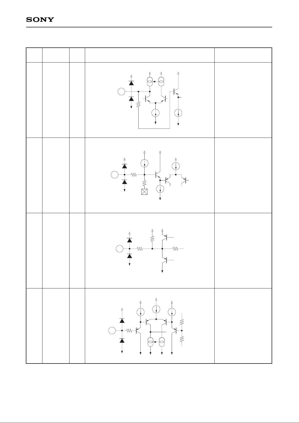
Pin Description
Pin
Symbol IO Equivalent circuit Description
No.
1
2
3
4
HOLD
AGCVTH
LD
PD
—
—
O
I
External hold timeconstant pin for RF
level control.
Variable pin of
reference level for RF
level control.
The reference level can
be varied by the
external resistor.
Output pin of APC
amplifier.
Input pin of APC
amplifier.
1k
10k
55.7k
V
CC VCC
VEE
3
147
50µ
10µ
13.4k
2
147
500µ
VEE
1
147
55k
10k
17µ
V
CC
VEE VEE VEE VEE
4

—4—
CXA2568M
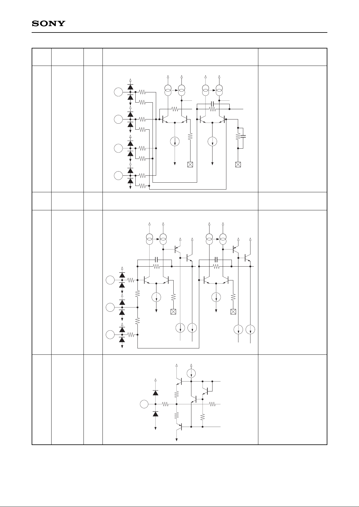
Pin
Symbol IO Equivalent circuit Description
No.
5
6
7
8
9
10
11
23
12
A
B
C
D
VEE
TE
E
LC/PD
VC
I
I
I
I
—
I
I
I
O
Input pin of RF and FE
amplifiers for Pins 5, 6,
7 and 8.
VEE.
Input pin of tracking
error amplifier for Pins
10 and 11.
An external resistor for
V-I conversion should
be connected because
these pins are for
current input.
Pin 23 is a bias for LC
when connected to VCC
and for PD IC when left
open.
DC voltage output pin of
(VCC+VEE)/2.
Connect to GND when
dual power supply (±2.5
V) is used; connect a
smoothing capacitor
when single power
supply (+5 V) is used.
A
24k
23.2k
B
24k
23.2k
C
24k
23.2k
D
24k
23.2k
14k
100µ
VC
4.2k
VEE
8µ
VEE
VCC VCC VCC VCC
174k
25p
VC
174k
25p
5
6
7
8
147
147
23
820k
820k
8µ
V
EE
VCC VCC
403k
12p
96.3k
VC
8µ
V
EE
96.3k
VC
VCC VCC
12p
VCC VCC
10
VCC VCC
11
403k
12
147
120
120
VCC
VEE
VCC
16k
15k
200µ

—5—
CXA2568M
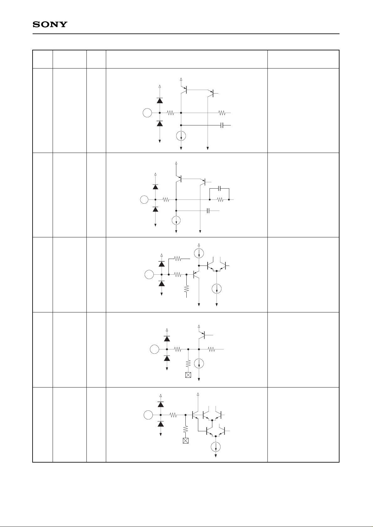
Pin
Symbol IO Equivalent circuit Description
No.
13
14
15
16
17
TE
FE
REF
RFO
RF_I
O
O
—
O
I
Output pin of tracking
error amplifier.
The F-E signal is
output.
Output pin of focus
error amplifier.
Equalizing pin of RF
amplifier.
Frequency response
can be adjusted by
connecting CR to this
pin.
Output pin of RF
amplifier.
Input pin of RF amplifier
output RFO with
capacitance coupled.
13
147 158.45k
10p
400µ
VEE VEE
VCC
147
400µ
VCC
VEE VEE
10p
174k
25p
14
5.7k
5k
25.4k
25µ
15
147
VCC
800µ
25.4k
60k
16
147
15k
20µ
17

—6—
CXA2568M
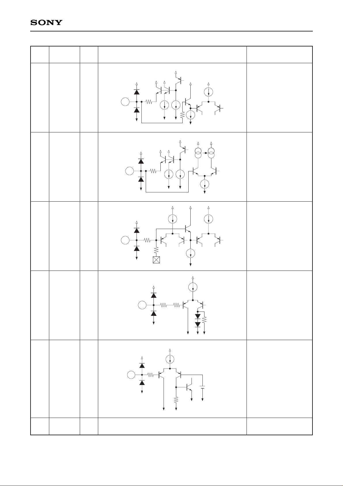
Pin
Symbol IO Equivalent circuit Description
No.
18
19
20
21
22
24
RFTC
RF_BOT
AGCCONT
HOLD_SW
LD ON
VCC
—
—
I
I
I
—
External time-constant
pin for RF level control.
External bottom timeconstant pin for RF
level control.
RF level control ON
(limit level of 60 % / 40
%)/ OFF switching pin.
60 % for VCC, 40 % for
open or VC and OFF for
VEE.
RF level control hold
ON/OFF switching pin.
ON for VCC and OFF for
VEE.
ON/OFF switching pin
of APC amplifier.
ON for VCC and OFF for
VEE.
VCC
147
50µ
10µ
50µ
18
147
50µ
50µ
19
20µ
147
15µ
7µ
50k
15µ
20
147
21
22
147
50µ
VEE VEE
30k
VEE VEE
VREF
V
CC
 Loading...