

Sony CXA2557R Datasheet

RF Amplifier for CD Player/CD-ROM
Description
The CXA2557R is an RF signal processing IC for
CD players, CD-ROM and CD-RW (playback).
Features
• Wide-band RF AC amplifier
• Supports CD-RW playback (RF DC, RF AC, FE,
TE and AL amplifiers)
• 5-mode RF AC equalizer (active filter type)
• RF AC equalizer boost amount and cut-off frequency
adjustable
• Voltage gain adjustable for RF DC, RF AC, FE, TE
and AL amplifier
• RF DC amplifier offset voltage switchable
• FE and TE amplifier bias voltage adjustable
• Tracking error amplifier cut-off frequency adjustable
• Alignment amplifier
• Center error amplifier
• AGC (Automatic Gain Control) function
• APC (Automatic Power Control) function
• VC/VC IN separation
• Supports laser coupler/3 spots
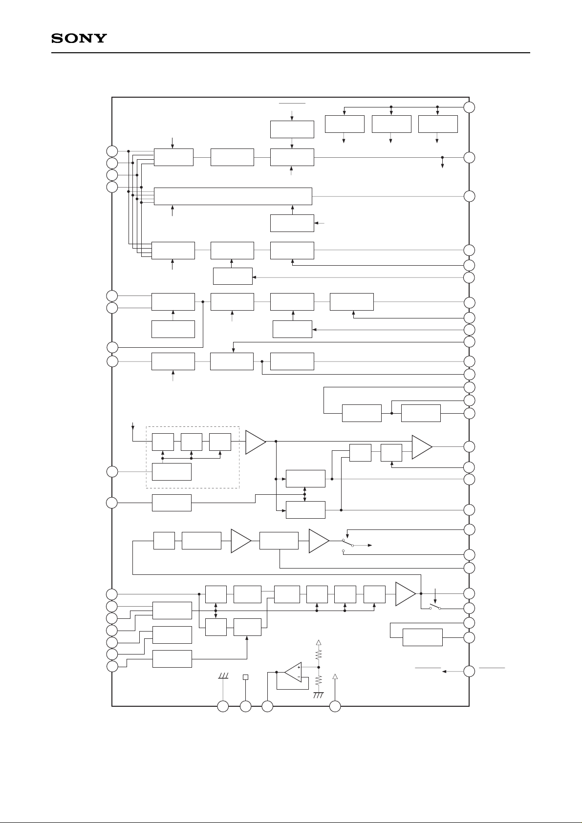
Functions
• RF DC summing amplifier
• RF AC summing amplifier
• RF AC equalizer
• Focus error (FE) amplifier
• Tracking error (TE) amplifier
• Alignment (AL) amplifier
• Center error (CE) amplifier
• Mirror circuit
• AGC circuit
• VREF output
Applications
• CD players
• CD-ROM drives
Structure
Bipolar silicon monolithic IC
Absolute Maximum Ratings (Ta = 25°C)
• Supply voltage VCC – GND 7 V
• Storage temperature Tstg –65 to +150 °C
• Power consumption PD 400 mW
Operating Conditions (Ta = 25°C)
• Supply voltage VCC – GND 3.5 to 5.5 V
• Operating temperature Topr –20 to +75 °C
– 1 –
E97757-PS
Sony reserves the right to change products and specifications without prior notice. This information does not convey any license by
any implication or otherwise under any patents or other right. Application circuits shown, if any, are typical examples illustrating the
operation of the devices. Sony cannot assume responsibility for any problems arising out of the use of these circuits.
CXA2557R
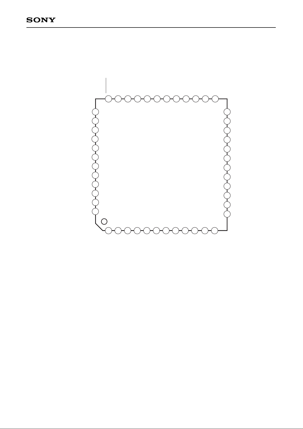
48 pin LQFP (Plastic)
For the availability of this product, please contact the sales office.
– 2 –
CXA2557R
2
7
8
9
10
11
12
14
15
16
17
18
20
21
22
25
26
27
28
29
30
40
39
37
36
31
32
33
41
46
48
1
PBH CNT
MIRR CNT
AL IN
TE 1
F
E
GND
VC IN
VC
V
CC
APC ON
LD
PD
RFO 2
RFO 1
HOLD C
VCA
AGC SW
BH C
MIRR
CE
CE 1
CE IN
AL 1
AL
AL CNT
TE CNT
TE BIAS
TE
FE
RF AC OUT
RF DC OUT
RW SW
APC ON
APC AMP
LPF 4
AMP
MODE 1
LPF 3LPF 2MIXERLPF 1
HPF BOOST
FC CNT
MODE CNT
BOOST
CNT
35
34
42
43
44
45
47
EQ IN
FC CNT 1
FC CNT 2
FC H CNT
MODE 1
MODE 2
BST CNT
HPF
PEAK
HOLD 1
AMP
PEAK
HOLD 2
COMP
VCA CNT
LPF 1
MIRR CNT
PBH CNT
PEAK
HOLD
BOTTOM
HOLD
LPF 2 LPF 3
LPF
RF DC OUT
AMP
COMP
HALF ADJ
23
24
PH C
MIRR BIAS
CE DRVCE AMP
AL DRVAL VCAAL AMP
RW SW 1
TE VCA
CNT
TE MODE
TE VCATE AMP
FE BIASFE VCA
TE RW AMP TE BIAS
RF AC VCA
FE VCA
CNT
RW SW 1
RW SW 1
19
38
FE CNT
FE BIAS
VCA CNT
RF AC SUM AMP
RW SW AC
RF DC VCA
RF DC
SUM AMP
RF DC AMP
RW SW DC
VCA CNT
RF DC OUT
DC OFFSET
APC ON
RF SW DC
RW SW DC
RW SW AC
RW SW AC
RW SW 1
RW SW 1
3
4
5
6
A
B
C
D
FE AMP
13
DELAY
Block Diagram
– 3 –
CXA2557R
AL CNT
40
TE CNT
39
FE CNT
38
MIRR CNT
37
VCA
41
BST CNT
42
FC H CNT
43
FC CNT 1
44
FC CNT 2
45
HOLD C
46
EQ IN
47
RF AC OUT
48
PD
2
A
3
B
4
C
5
D
6
GND
7
E
8
F
9
TE 1
10
AL IN
11
AL
12
AL 1
13
CE IN
14
CE 1
15
CE
16
TE
17
TE BIAS
18
FE BIAS
19
FE
20
PBH CNT
21
BH C
22
PH C
23
MIRR BIAS
24
MODE 2
35
MODE 1
34
V
CC
31
RW SW
32
AGC SW
33
MIRR
25
RF DC OUT
26
VC IN
27
VC
28
RFO 1
29
RFO 2
30
LD
1
APC ON
36
Pin Configuration
– 4 –
CXA2557R
Pin Description
Pin
No.
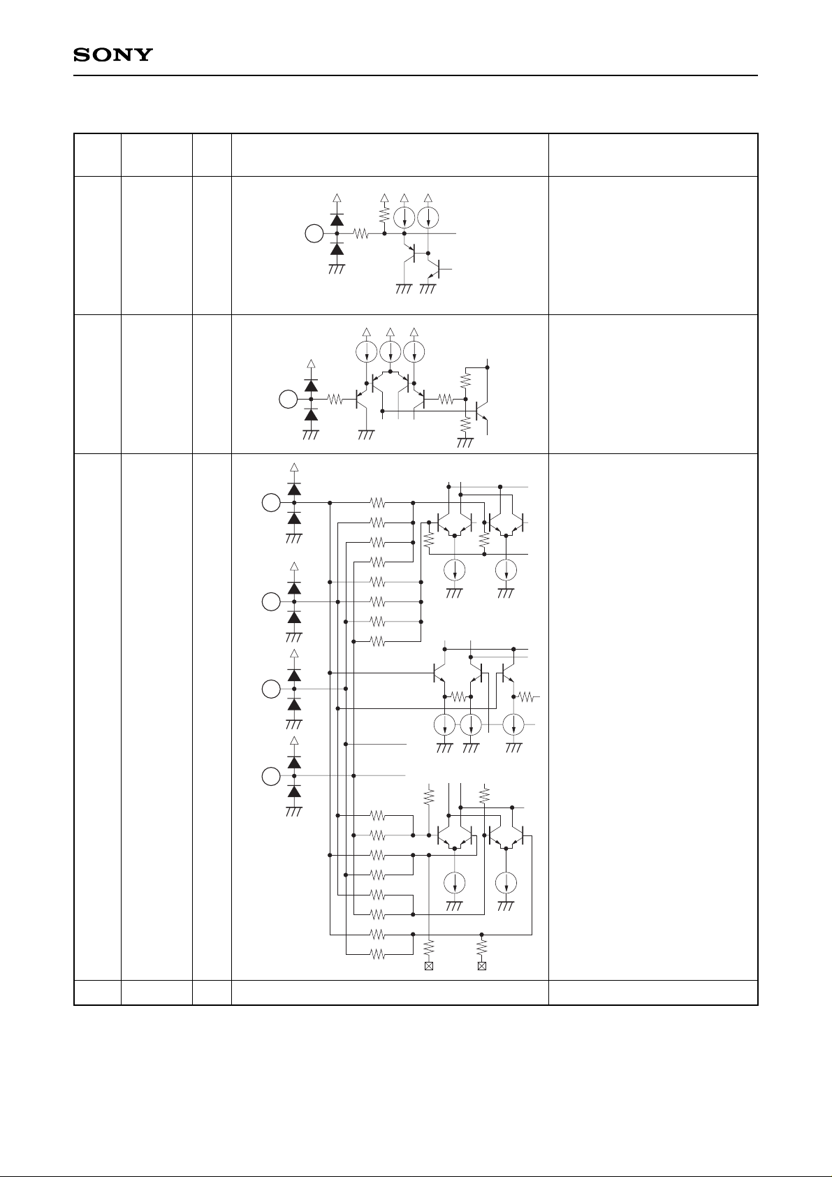
1 LD APC amplifier output.
APC amplifier input.
Inputs of RF summing amplifier
and focus error amplifier.
When using a laser coupler:
A + C = PD1
B + D = PD2
Ground.
O
I
I
I
I
I
PD
A
B
C
D
GND
2
3
4
5
6
7
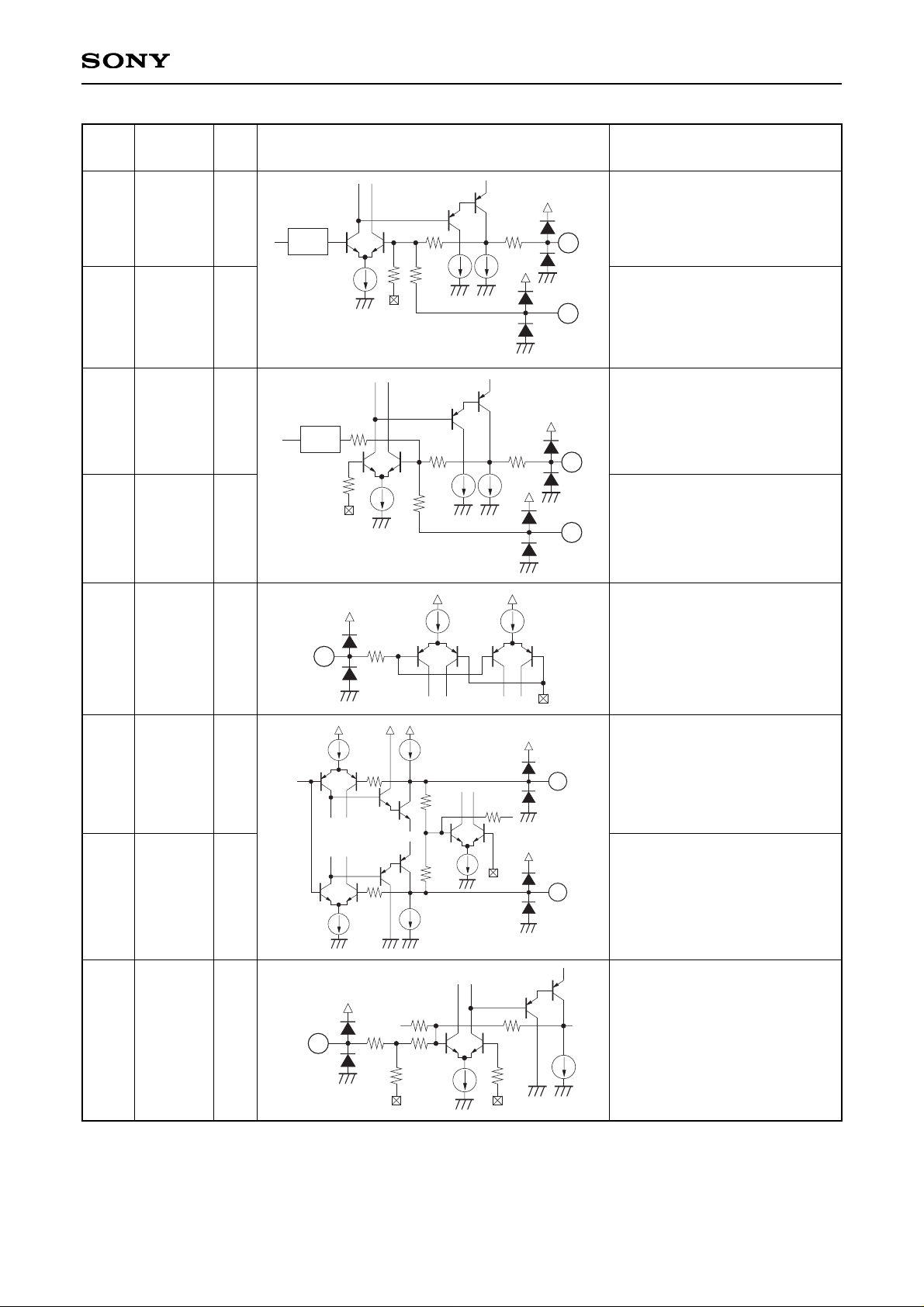
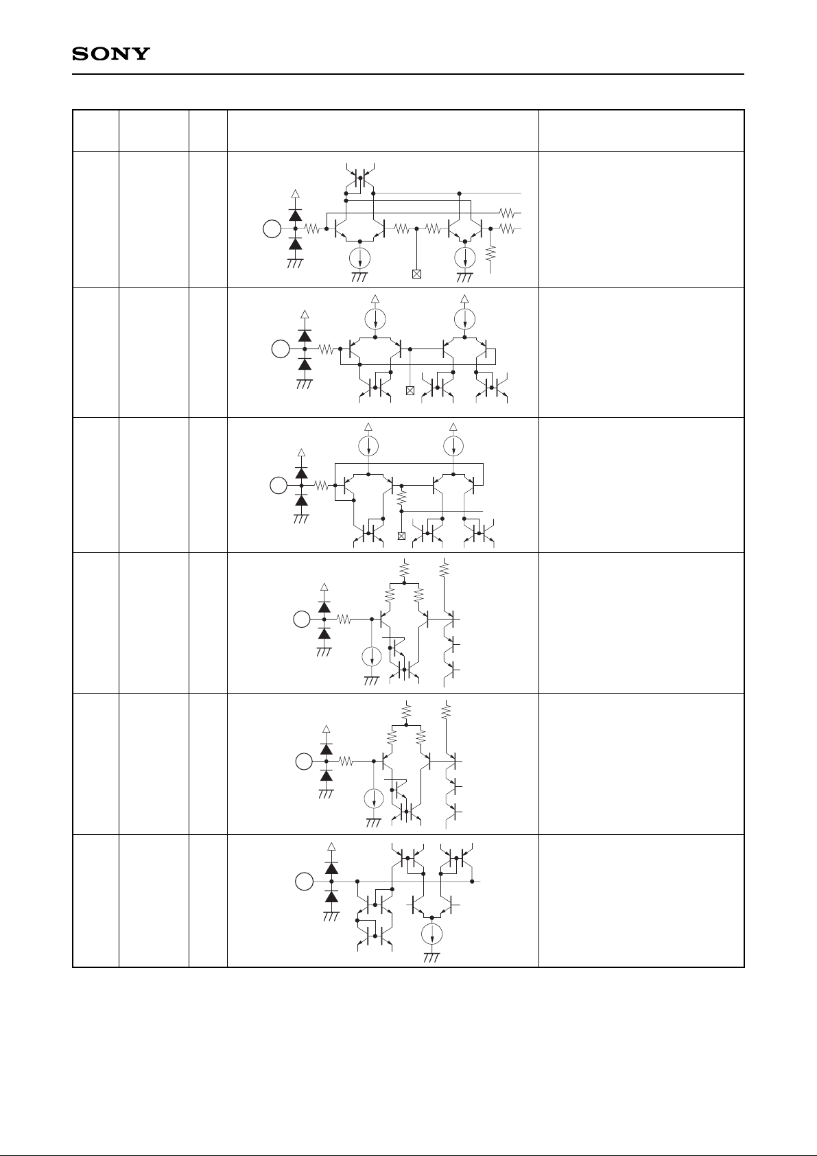
Symbol I/O Equivalent circuit Description
1
10k
124
20k
124
2
20k
55k
10k345k
40k
40k
40k
40k
40k
40k
40k
40k
4
5
6
130k
40k
40k
40k
40k
180k
180k
180k
180k
130k
130k 130k
—
– 5 –
CXA2557R
11
AL IN
Alignment amplifier input.
I
124
40k
20k
13.3k
6.2k
20k
9k
11
12 AL
Alignment amplifier non-inverted
output.
O
124
15k
15k
12
7.5k
124
34k
45k
13
124
124
15
14
124
20k
16
13 AL 1
Alignment amplifier inverted
output.
14 CE IN Center error amplifier input.
15 CE 1
Center error amplifier inverted
output.
16
CE
I
O
O
Center error drive amplifier
inverted output.
O
Tracking error amplifier inputs.
Tracking error amplifier inverted
output.
I
I
O
E
F
8
9
TE 1
10
124
124
8
124
9
10
VCA RW
Pin
No.
Symbol I/O Equivalent circuit Description
– 6 –
CXA2557R
19 FE BIAS I
Focus error amplifier bias
adjustment.
20 FE O
Focus error amplifier noninverted output.
124
107k
300k
20
VCA
300k
375k
19
21
PBH
CNT
I
Mirror circuit peak hold and
bottom hold time constant
setting input.
50k
21
22 BC C I
Connects the capacitor that
sets mirror circuit bottom hold
time constant.
23 PH C I
Connects the capacitor that sets
mirror circuit peak hold time
constant.
22
23
40k
40k
500
500
20k
24
MIRR
BIAS
I Mirror circuit bias adjustment.
2.7k
35k
3k
20k
20k
50k
24
17 TE O
Tracking error amplifier noninverted output.
18 TE BIAS
I
Tracking error amplifier bias
adjustment.
124
200k
17
18
50k
40k
VCA
Pin
No.
Symbol I/O Equivalent circuit Description
– 7 –
CXA2557R
28 VC
(VCC + GND)/2 voltage output.
O
28
150
150
29 RFO 1 O RF AC amplifier output.
30
RFO 2
O
RF AC amplifier buffer switch
output.
ON when Pin 34 is connected
to GND.
3k
280
3k 3k
280
3k
29
30
25
MIRR
O
Mirror comparator output.
2k
7.7k
8k
200k
124
25
26
RF DC
OUT
O
RF DC amplifier output.
Eye pattern check point.
27 VC IN
I
Reference voltage input.
20k
26
20k
20k
31 VCC
—
Power supply.
—
—
Pin
No.
Symbol I/O Equivalent circuit Description
– 8 –
CXA2557R
34
MODE 1
Double-speed mode switching
pins.
n is determined by the external
resistor connected to Pin 44.
N is determined by the external
resistor connected to Pin 45
and the Pin 43 input voltage.
Pin 34 also serves as switching
pin for the tracking error
amplifier cut-off frequency and
RFO2 output ON/OFF switching
pin.
I
15k
40k
124
34
80k
15k
15k
15k
40k
80k
15k
15k
40k
80k
15k
15k
40k
80k
35
MODE 1 MODE 2 fc
L
M
H
X
L
M
H
X
× n
× 2n
× 4n
× 6n
× N
∗
X = L or M or H
MODE 1 MODE 2 fc
L
M
H
20kHz
250kHzONOFF
∗
L = GND, M = VC, H = VCC
35 MODE 2 I
33
AGC
SW
AGC/VCA switching input.
AGC when connected to VCC,
VCA when connected to GND.
I
15k
15k
20k 60k
33
32
RW SW
I
CD-ROM/RW switching input.
RW when connected to VCC,
ROM when connected to GND.
15k
15k
40k
20k
20k
20k 60k
80k
124
32
15k
15k
40k 80k
Pin
No.
Symbol I/O Equivalent circuit Description
– 9 –
CXA2557R
Switching pin for RF DC
amplifier offset setting.
No addition to RF DC amplifier
when Medium (VC).
VCC/6 added to RF DC amplifier
when Low (GND).
10k
80k
20k
40k
80k
40k
10k
124
40k
100k
36
36
APC ON
I
37
MIRR
CNT
I
Mirror circuit LPF cut-off
frequency setting input.
12k
12k
37
38 FE CNT I
Focus error amplifier gain
adjustment input.
21k
21k
38
39 TE CNT I
Tracking error amplifier gain
adjustment input.
21k
21k
39
40 AL CNT I
Alignment amplifier gain
adjustment input.
21k
21k
40
Pin
No.
Symbol I/O Equivalent circuit Description
– 10 –
CXA2557R
44
FC CNT
1
I
Connects the external resistor
that sets cut-off frequency n
when Pin 34 is Low or Medium.
124
15k5k
5k5k
44
45
FE CNT
2
I
Connects the external resistor
that sets cut-off frequency N
when Pin 34 is High.
124
15k5k
5k5k
45
46
HOLD C
I
Connects the capacitor that
sets AGC time constant.
46
42
BST
CNT
I
Equalizer circuit boost amount
adjustment input.
20k
42
43
FC H
CNT
I
Cut-off frequency N adjustment
input when Pin 34 is High.
20k
20k
43
41
VCA
I
RF DC and RF AC amplifier
gain adjustment input.
AGC circuit target voltage input
when AGC SW is ON.
80k
40k
40k 26.7k 80k
80k
41
Pin
No.
Symbol I/O Equivalent circuit Description
– 11 –
CXA2557R
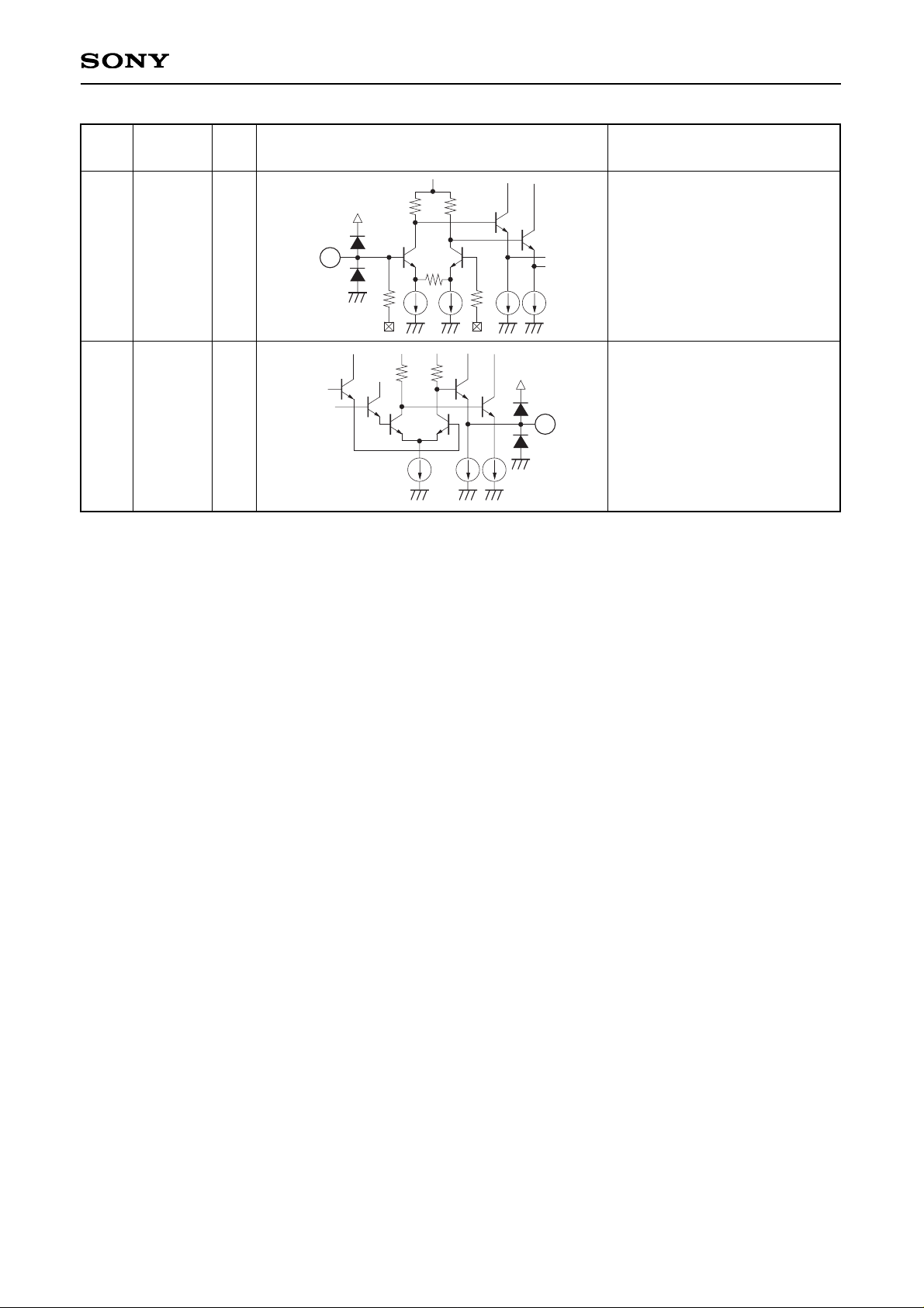
47
EQ IN
I
Equalizer circuit input.
1.1k
1.1k
5k
1.3k
5k
47
48
RF AC
OUT
O
RF AC summing amplifier noninverted output.
3k
3k
48
Pin
No.
Symbol I/O Equivalent circuit Description
 Loading...