

Sony CXA2556Q Datasheet

RF Amplifier for CD Player/CD-ROM
For the availability of this product, please contact the sales office.
Description
The CXA2556Q is an IC for RF signal processing of
CD player and CD-ROM.
Features
• Wide-band RF AC amplifier
(RF AC signal fc ≥ 20MHz)
• 4-mode RF equalizer (active filter type)
• RF equalizer boost amount and cut-off frequency
adjustable
• EFM time constant adjustable (switching function
provided)
• Peak hold time constant of mirror circuit adjustable
• Tracking error amplifier cut-off frequency adjustable
• Tracking error amplifier voltage gain adjustable
• APC (Automatic Power Control) function
• APC ON/OFF control
Absolute Maximum Ratings
• Supply voltage VCC 7V
•Storage temperature Tstg –65 to +150 °C
• Power consumption PD 800 mW
Applications
• CD players
• CD-ROM drives
Functions
• RF summing amplifier
• RF equalizer
• Focus error amplifier
• Tracking error amplifier
• Mirror detection function
• APC circuit
CXA2556Q
32 pin QFP (Plastic)
Operating Conditions
• Supply voltage VCC – GND 3.0 to 5.5 V
• Operating temperature Topr –20 to +75 °C
Sony reserves the right to change products and specifications without prior notice. This information does not convey any license by
any implication or otherwise under any patents or other right. Application circuits shown, if any, are typical examples illustrating the
operation of the devices. Sony cannot assume responsibility for any problems arising out of the use of these circuits.
– 1 –
E96731B76
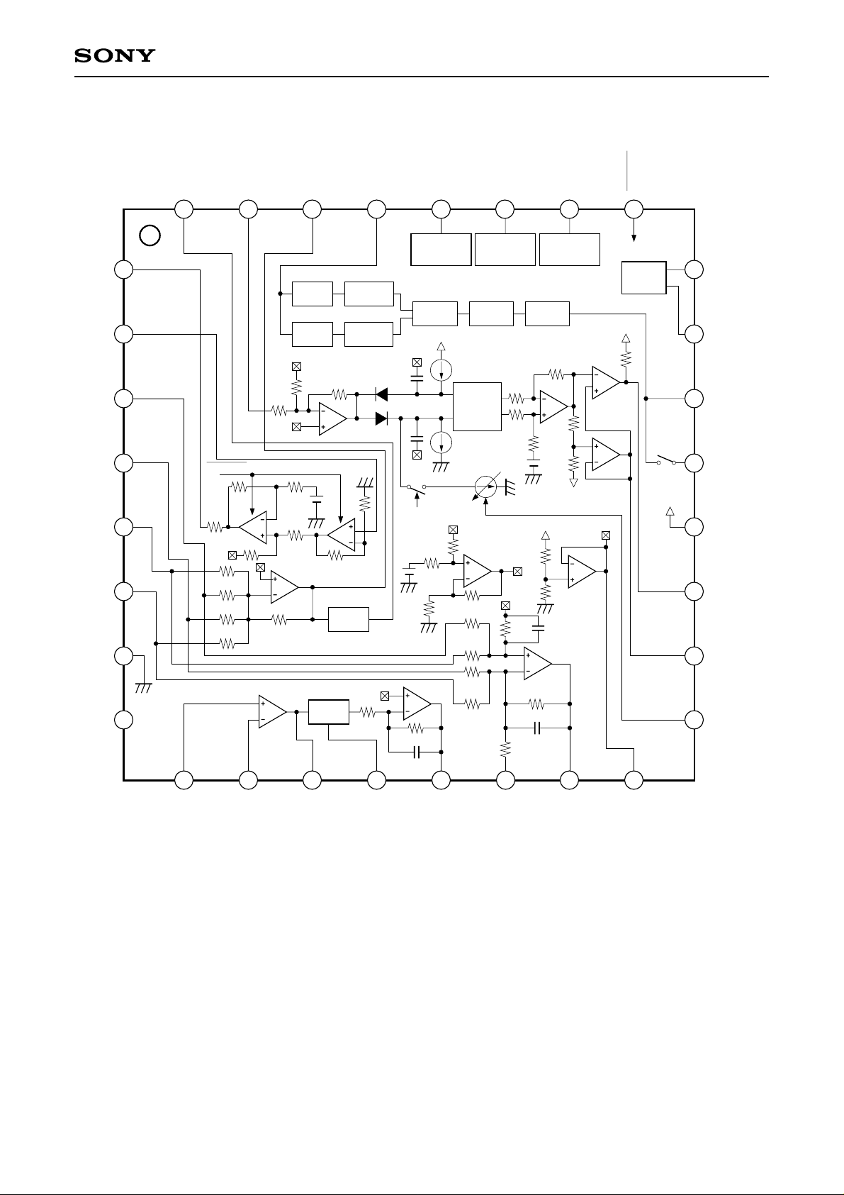
Block Diagram
CXA2556Q
LD
PD
GND
FC C
2627
FILTER
CONTROL
80k
22k
51k
VCC
VCC
27p
20k
VC
25
MODE
Vcc
APC ON
SW
VCC
24
23
22
21
20
19
18
MODE 1
MODE 2
RFO 1
RFO 2
V
CC
MIRR
CP
10k
EQ IN
29
44p
Open only for
L/L mode
RF C
28
VCA
CONTROL
MIXER LPF VCA
VCC
VC
HOLD
PEAK
40k
/BOT
VC
20k
32k
32k
10p
VC
1.25V
40k
BST C
BOOST
CONTROL
80k
80k
80k
1.3V
VS
20k
VC
87k
40k
40k
RFO
32
1
2
A
3
4
B
5
C
6
D
7
APC ON
VC
RFI
31
56k 10k
1k
56k
40k
40k
40k 10k
40k
18k
VC
VC
SUM OUT
30
LPF DELAY
HPF BOOST
VS
39k
44k
1.25V
10k
55k
VCA
NC
8
GND
VC
VCA
73.34k
320k
2p
9
E
10
11
F
TE1
12
TE C
32k
32k
164k
13
TE
14
FE B
174k
27p
15
FE
16
VC
17
MIRR T
– 2 –
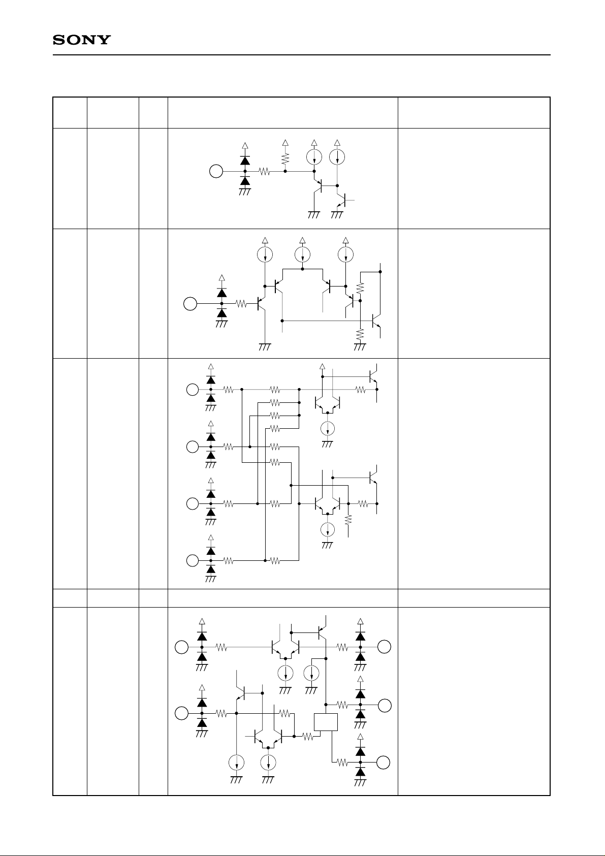
Pin Description
CXA2556Q
Pin
No.
Symbol I/O Equivalent circuit Description
10k
1 LD APC amplifier output.
PD
2
A
3
B
4
C
5
D
6
O
I
I
I
I
I
1
2
3
4
147
147
8k
855
32k
32k
40k
40k
40k
40k
10k
10k
55k
APC amplifier input.
Input of RF summing amplifier
and focus error amplifier.
5
147
32k
174k
164k
7
9
10
11
12
13
GND
E
F
TE1
TE C
TE
6
147
32k
Ground.
9
147
147
10
Tracking error amplifier input for
I
I
O
13
I
160k147
O
36.7k
147
VCA
147
Pins 9 and 10; tracking error
amplifier output for Pin 11;
tracking error amplifier low-
11
frequency gain setting for Pin
12; tracking error amplifier
output for Pin 13.
12
– 3 –

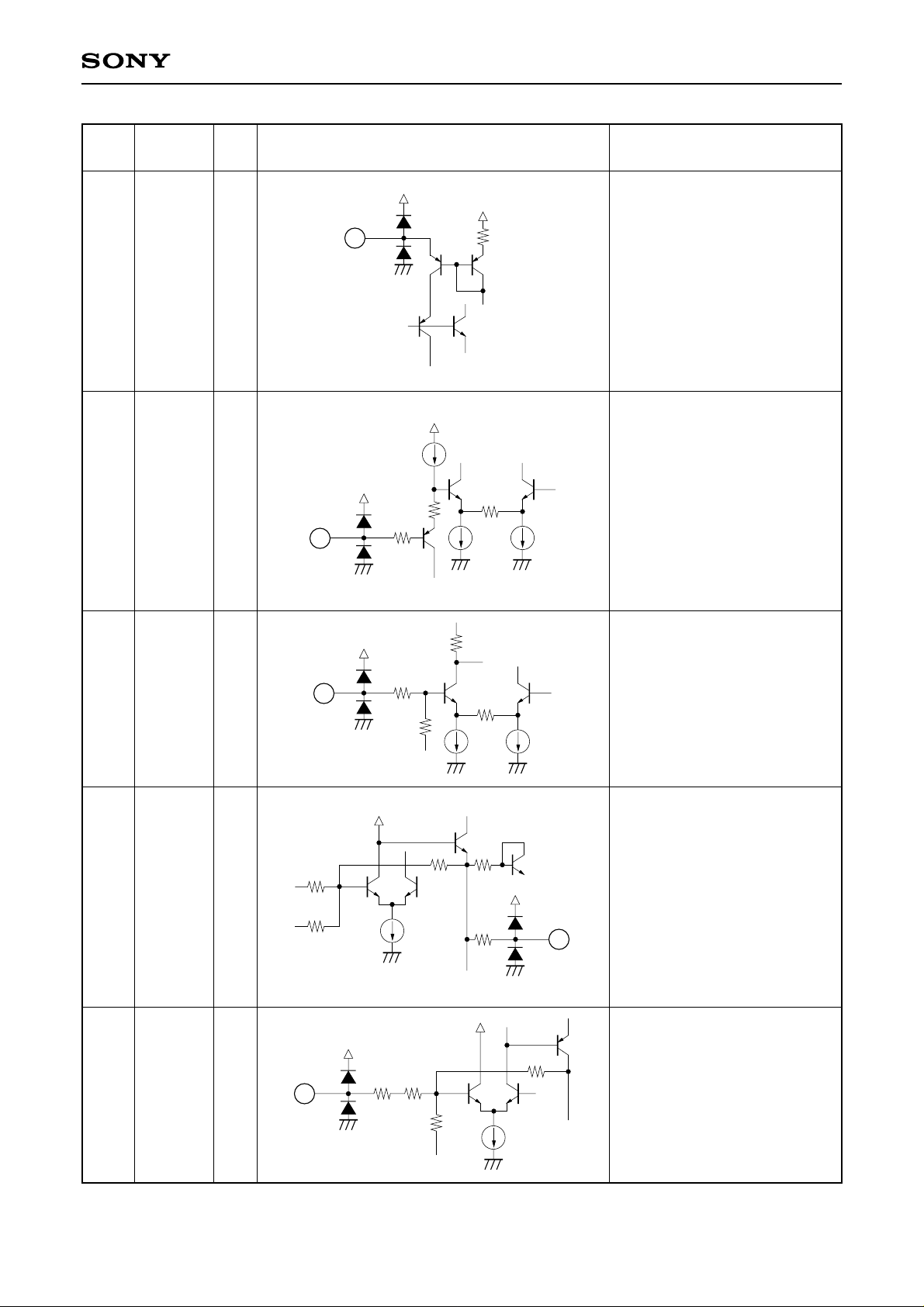
CXA2556Q
Pin
No.
8
14
15
16
Symbol I/O Equivalent circuit Description
NC
FE B
FE
VC
147
164k
14
O
O
174k
120
O
120
147
15
16
Not connected.
Focus bias adjustment for Pin
14; focus error amplifier output
for Pin 15.
(Vcc + GND)/2 DC voltage
output.
17 MIRR T
18 CP
19 MIRR Mirror comparator output.O
VCC
147
I
17
I
120k 80k
80k1.5k
147
10k
10k
Peak hold time constant
adjustment.
Connects a mirror hold
capacitor.
Non-inverted input of mirror
comparator.
18
20k
40k
147
19
100k
– 4 –

CXA2556Q
Pin
No.
Symbol I/O Equivalent circuit Description
VCC Power supply.
20
2122RFO 2
RFO 1
23 MODE 2 I
3k
147
21
O
O
147
22
Buffer switch output for the RF
time constant setting for Pin 21.
ON when Pins 23 and 24 are
connected to GND.
RF equalizer output.
Double-speed mode switching
input.
147
23
10k
40k
× 1
× N
× 1.5N
Mode 1 Mode 2
GND
VCC
GND
GND
GND
VCC
24 MODE 1 I
25 APC ON I
26
FC C I
24
25
5k
147 10k
147
5k5k
147
100k
40k
26
× 2.0N
VCC
VCC
N is varied according to the
external resistor connected to
Pin 26.
Switching pin for APC amplifier
ON/OFF.
OFF when connected to Vcc;
ON when connected to GND.
Input to set the RF equalizer
LPF cut-off frequency.
– 5 –
CXA2556Q
Pin
No.
Symbol I/O Equivalent circuit Description
27 BST C
28 RF C
27
I
I
28
10k
147
5k
Sets the high-frequency boost
amount of RF equalizer.
Sets the low-frequency gain of
RF amplifier and RF equalizer.
29 EQ IN RF equalizer input.I
SUM
30
OUT
31 RFI
430
29
20k
O
20k
I
31
147
10k
147 18k
44k
2k
10k
RF summing amplifier output
inversion.
147
30
39k
Mirror circuit input.
The RF summing amplifier
output is input.
– 6 –

CXA2556Q
Pin
No.
Symbol I/O Equivalent circuit Description
32 RFO
15k
O
15k
147
32
RF signal output.
Eye pattern check point.
– 7 –
 Loading...