


CXA2543R
Decoder/Driver/Timing Generator for Color LCD Panels
Description
The CXA2543R is an IC designed exclusively to
drive the color LCD panel DCX501BK and LCX018AK.
This IC greatly reduces the number of circuits and
parts required to drive LCD panels by incorporating
RGB decoder functions for video signals, driver
functions, and a timing generator for driving panels
onto a single chip.
This chip has a built-in serial interface circuit and
electronic attenuators which allow various mode
settings and adjustments to be performed through
direct control from an external microcomputer, etc.
Features
• Color LCD panel DCX501BK and LCX018AK driver
• Supports NTSC and PAL signals
• Supports 16:9 wide display
• Supports composite inputs, Y/C inputs and Y/color
difference inputs
• Serial interface circuit
• Electronic attenuators (D/A converter)
• BPF, trap and delay line
• Sharpness function
• 2-point γ correction circuit
• R, G, B signal delay time adjustment circuit
• Polarity inversion circuit (line inverted mode)
• Supports external RGB input
• Supports AC drive for LCD panel during no signal
Applications
• Compact LCD monitors
• LCD viewfinders
• Compact liquid crystal projectors, etc.
Structure
Bipolar CMOS IC
Absolute Maximum Ratings (Ta = 25°C)
• Supply voltage VCC1 – GND1 6 V
VCC2 – GND2 14 V
VCC3 – GND3 14 V
VDD1 – VSS1 4.5 V
VDD1 – VSS2 4.5 V
• Analog input pin voltage VINA –0.3 to VCC V
• Digital input pin voltage VIND –0.3 to VDD1 + 0.3V
• Operating temperature Topr –15 to +75 °C
• Storage temperature Tstg –40 to +125 °C
• Allowable power dissipation
∗1
PD (Ta ≤ 75°C) 350 mW
Operating conditions
Supply voltage VCC1 – GND1 4.25 to 5.25 V
VCC2 – GND2 11.0 to 13.5 V
VCC3 – GND3 11.0 to 13.5 V
VDD1 – VSS1 2.7 to 3.6 V
VDD1 – VSS2 2.7 to 3.6 V
∗1
With substrate Size: 30 × 30 × 1.6mm
Material: Glass fabric base epoxy
– 1 –
E98403-PS
Sony reserves the right to change products and specifications without prior notice. This information does not convey any license by
any implication or otherwise under any patents or other right. Application circuits shown, if any, are typical examples illustrating the
operation of the devices. Sony cannot assume responsibility for any problems arising out of the use of these circuits.
64 pin LQFP (Plastic)
– 2 –
CXA2543R
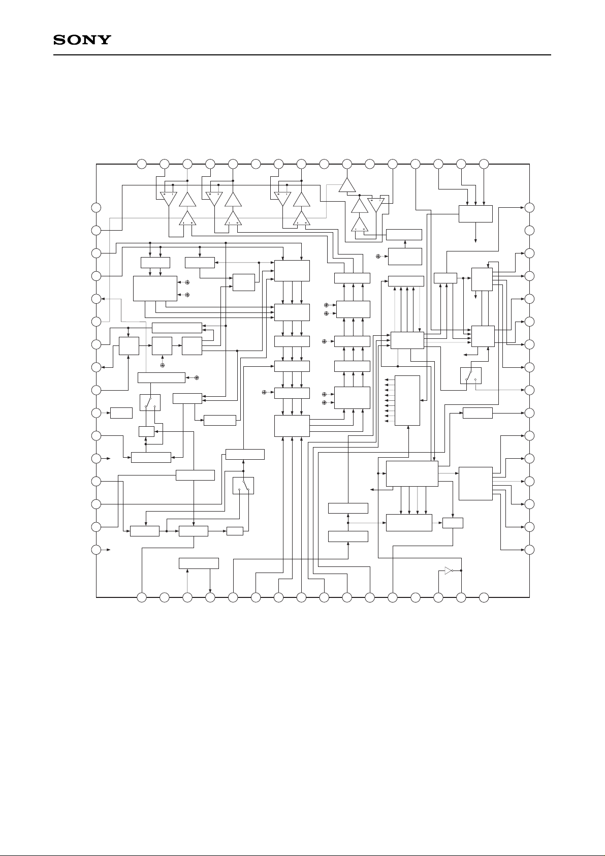
Block Diagram
POL SW
SUBBRIGHT
GAMMA
DEMOD
LPF
CONTRAST
EXT SW
BRIGHT
S/H
INT/EXT
VXO HUE PS
KILLER
FILT ADJ
COLOR CONT
BPF
PIC CONT
DL1
TRAP
CLAMP
ACC AMP
H. FILTER
Buf
REG.
R G B
+12V
+12V
GND1
V
SS1
+4.5V
Buf Buf
PAL
SW
EXT COLOR
& BALANCE
HUE
HUE
COLOR
CONTRAST
R-BRT
B-BRT
γ -1
γ -2
SERIAL
BUS I/F
VSS2
VGATE
VTST
VPAL
VWIN
WIDE
PALSW
D/A
HCNT
H-PULSE
HAFC
PLL-COUNTER
& DECODER
HGATE
H-SKEW DET
PD
CLP
BGP
SBLK
V SEP
+3V
MATRIX
Buf
Buf
POL SW
PSIGBRIGHT
PSIG-BRT
APC
ACC DET
HD
GND3
GND2
SYNC SEP
FRP
COLOR
PAL IDCLAMP
VD
V
SS2
EN
XEN
VCK1
VCK2
VST
XVST
FLD IN
HD
PCG
XPCG
HCK1
HCK2
HST
XHST
46
40
39
38
37
36
35
34
33
41
42
43
44
45
47
48
49
50
51
52
53
54
55
56
57
58
59
60
63
64
61
62
17
18
19
20
21
22
23
24
25
26
27
28
29
30
31
32
2
3
4
5
6
7
8
9
10
11
12
13
14 15
16
1
V
DD
1
CKO
CKI
V
SS
1
RPD
TEST2
EXT B
EXT G
EXT R
S.SEP IN
H.FIL OUT
SYNC IN
GND1
TRAP
TEST1
VD IN
VCC1
SIG. CENTER
B-Y IN
R-Y IN
BLK LIM
APC
VXO OUT
VXO IN
V REG
C IN
TEST3
Y IN
PIC
PWRST
F0 ADJ
C OUT
SCLK
DATA
LOAD
RGT
FB PSIG
GND3
PSIG
V
CC
3
B OUT
FB B
G OUT
FB G
R OUT
FB R
V
CC
2
GND2
BRIGHT
– 3 –
CXA2543R
Pin Description
Pin
No.
1
2
3
4
5
6
7
8
9
10
11
12
13
14
15
16
17
18
19
20
21
22
23
24
25
26
27
28
29
30
31
32
TRAP
GND1
SYNC IN
H.FIL OUT
S.SEP IN
EXT R
EXT G
EXT B
VD IN
TEST1
TEST2
RPD
VSS1
CKI
CKO
VDD1
XHST
HST
HCK2
HCK1
XPCG
PCG
HD
FLD IN
XVST
VST
VCK2
VCK1
XEN
EN
VSS2
VD
Symbol
H
H
I
O
I
I
I
I
I
O
I
O
O
O
O
O
O
O
O
I
O
O
O
O
O
O
O
External trap connection
Analog (4.5V) GND
Video input for sync separation
Video output for sync input
Sync separation circuit input
External digital input R
External digital input G
External digital input B
External vertical sync input
Test (Leave this pin open.)
Test (Leave this pin open.)
Phase comparator output
Digital (3V) GND for oscillation cell
Oscillation cell input
Oscillation cell output
Digital 3V power supply
XH start pulse output (HST reversed polarity)
H start pulse output
H clock pulse 2 output
H clock pulse 1 output
XPCG pulse output (PCG reversed polarity)
PCG pulse output
HD pulse output
Field identification input
XV start pulse output (VST reversed polarity)
V start pulse output
V clock pulse 2 output
V clock pulse 1 output
XEN pulse output (EN reversed polarity)
EN pulse output
Digital (3V) GND
VD pulse output
I/O Description
Input pin
for open
status
(H: Pull up)
– 4 –
CXA2543R
33
34
35
36
37
38
39
40
41
42
43
44
45
46
47
48
49
50
51
52
53
54
55
56
57
58
59
60
61
62
63
64
H
H
H
H
SCLK
DATA
LOAD
RGT
FB PSIG
GND3
PSIG
VCC3
B OUT
FB B
GND2
G OUT
FB G
R OUT
FB R
VCC2
VCC1
SIG.CENTER
B-Y IN
R-Y IN
C OUT
BLK LIM
APC
VXO OUT
VXO IN
V REG
C IN
TEST3
Y IN
PIC
F0 ADJ
PWRST
I
I
I
I
O
O
O
O
O
O
O
O
I
I
I
O
I
O
O
I
O
I
I
I
I
O
—
Serial interface clock input
Serial interface data input
Serial interface load input
Switches between Normal scan (H) and Reverse scan (L)
PSIG signal DC voltage feedback circuit capacitor connection
Analog (12V) GND for PSIG
PSIG output
Analog 12V power supply for PSIG
B signal output
B signal DC voltage feedback circuit capacitor connection
Analog (12V) GND
G signal output
G signal DC voltage feedback circuit capacitor connection
R signal output
R signal DC voltage feedback circuit capacitor connection
Analog 12V power supply
Analog 4.5V power supply
R, G, B and PSIG output DC voltage adjustment
B-Y demodulator input (or B-Y color difference signal input)
R-Y demodulator input (or R-Y color difference signal input)
Chroma signal output
Black peak limiter level adjustment
APC detective filter connection
VXO output
VXO input
Constant voltage capacitor connection
Chroma signal input
Test (Connect to GND.)
Y signal input
Y signal frequency response adjustment
Internal filter adjusting resistor connection
System reset
(H: Pull up)
Pin
No.
Symbol I/O Description
Input pin
for open
status
– 5 –
CXA2543R
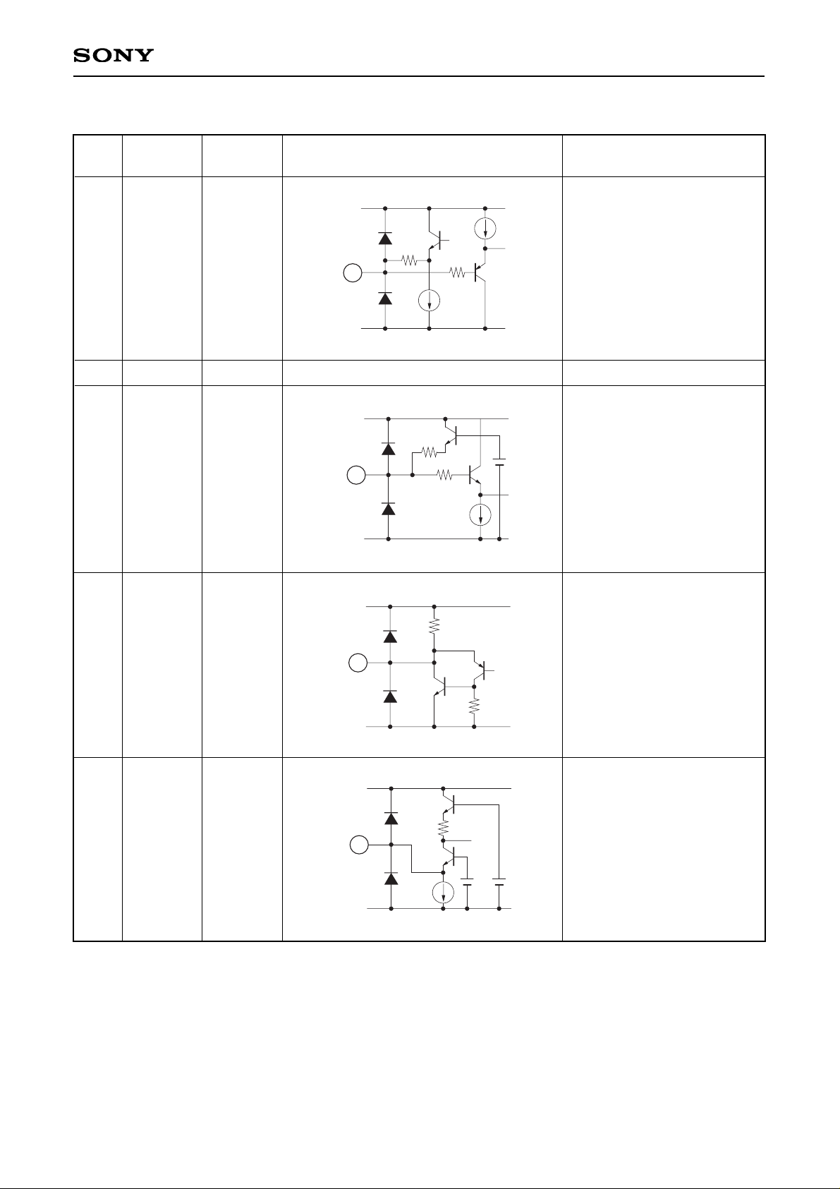
Analog Block Pin Description
Pin
No.
Symbol Pin voltage Equivalent circuit Description
1 TRAP —
2 GND1
0V
Analog (4.5V) GND.
VCC1
GND1
130µA
1k
300
70µA
1
External trap connection.
Connect the trap between this
pin and GND to remove the
chroma component.
Leave this pin open when
using Y/C and Y/color
difference input.
3 SYNC IN 1.5V
Sync input.
Normally inputs the Y signal.
The standard signal input level
is 0.5Vp-p (100% white level
from the sync tip).
VDD1
GND1
1k
30µA
3
2.1V
1k
4 H.FIL OUT 0.8V
Outputs the video signal for
input to the sync separation
circuit.
VDD1
GND1
20k
20k
4
5 S.SEP IN
2.1V
Sync separation circuit input.
Input the H.FIL OUT (4pin)
signal.
VDD1
GND1
17k
1.8V10µA 2.8V
5
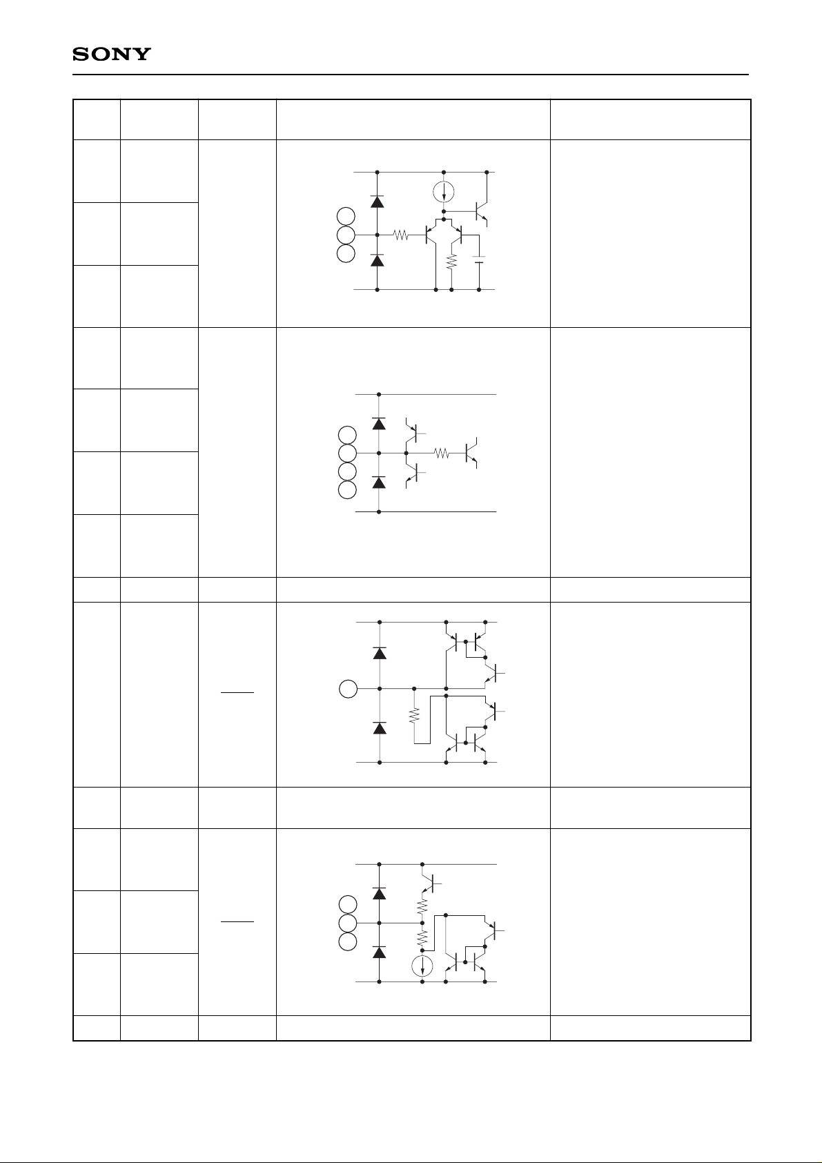
– 6 –
CXA2543R
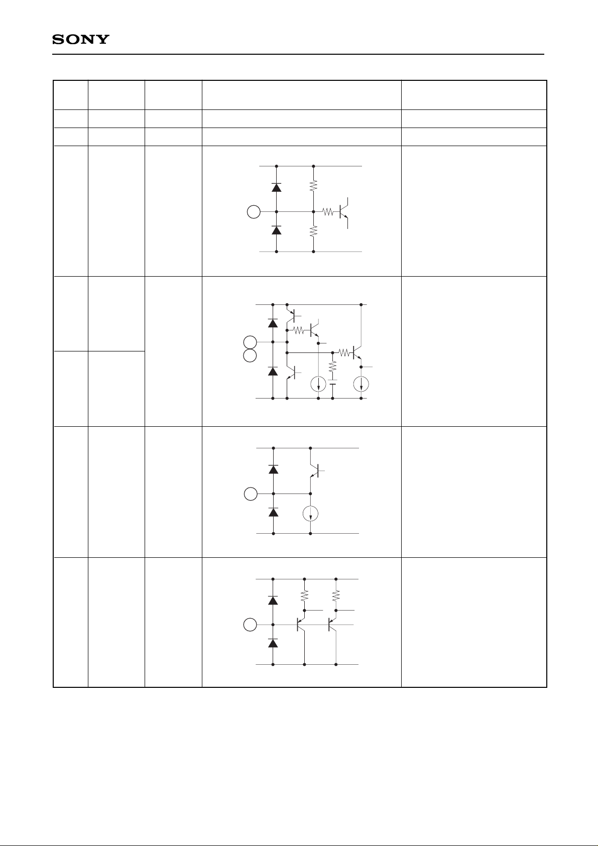
6 EXT-R
7 EXT-G
8 EXT-B
42 FB B
37 FB PSIG
45 FB G
47 FB GR
41 B OUT
44 G OUT
46 R OUT
External digital signal inputs.
There are two threshold
values: Vth1 (= 1.0V) and
Vth2 (= 2.0V). When one of
the RGB signals exceeds
Vth1, all of the RGB outputs
go to black level; when an
input exceeds Vth2, only the
corresponding output goes to
white level.
6
8
300
VCC1
GND1
30µA
50k
2.7V
7
Smoothing capacitor
connection for the feedback
circuit of R, G, B and PSIG
output DC level control.
Use a low-leakage capacitor
because of high impedance.
1k
VCC1
GND2
42
37
45
47
—
VCC2
2
RGB signal outputs.
46
VCC2
GND2
40µA
20
20
44
41
2.0V
38 GND3
0V
Analog (12V) GND for the PSIG circuit.
PSIG signal outputs.
VCC3
GND3
10
39
39 PSIG
VCC2
2
40 VCC3
12V
12V power supply for the PSIG
circuit.
43
GND2
0V
Analog (12V) GND.
Pin
No.
Symbol Pin voltage Equivalent circuit Description
– 7 –
CXA2543R
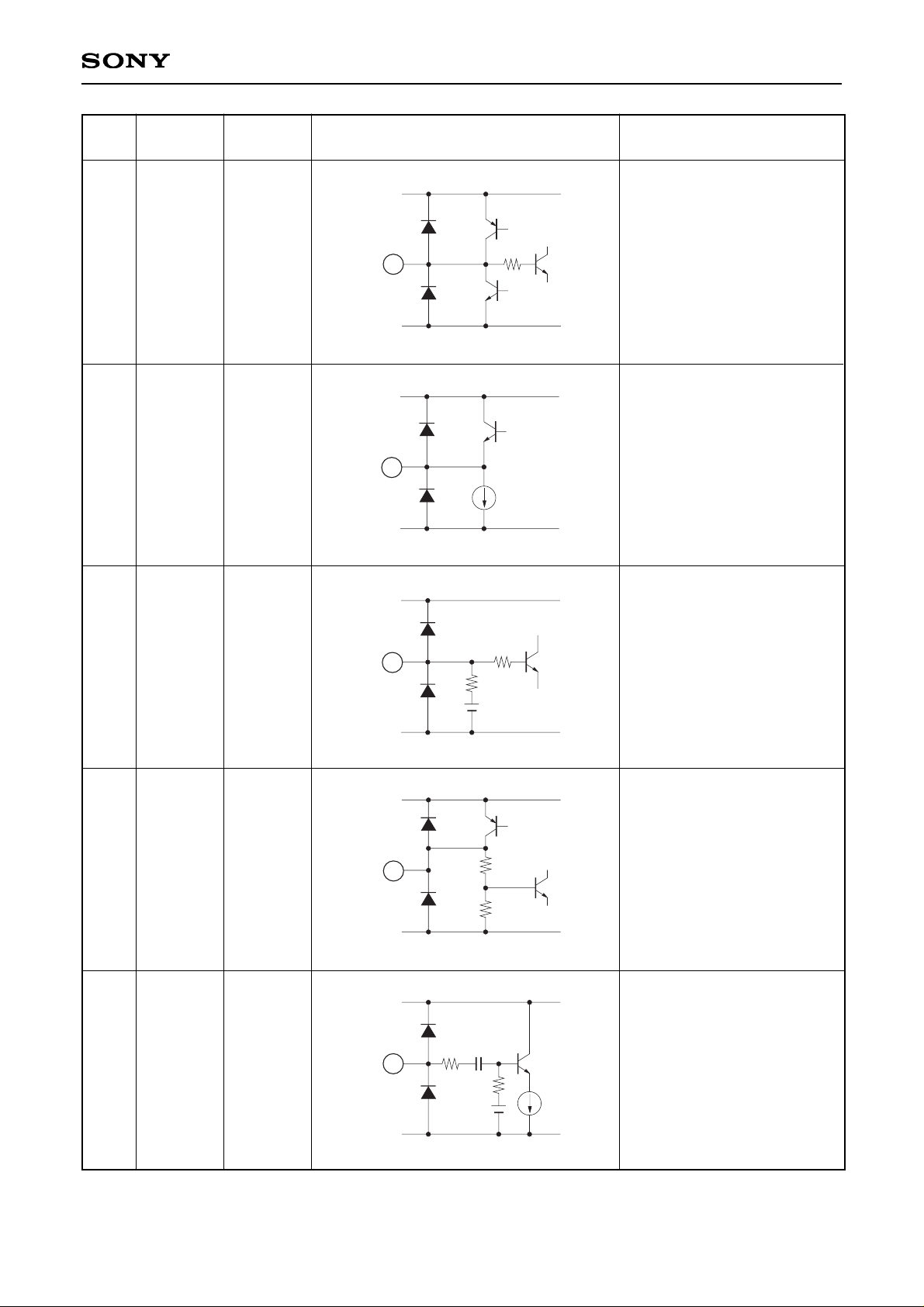
51
B-Y IN
52 R-Y IN
—
Color difference demodulation
circuit inputs.
Color difference signal is input
when using Y/color difference
input. At this time, the
standard signal input level is
0.3Vp-p and the clamp level is
approximately 2.8V. Pin 53
signal is input in other modes
(except D-PAL∗). At this time,
the DC level is approximately
1.6V.
500
GND1
10k
30µA
50µA
VCC1
500
52
51
50
SIG.
CENTER
6.0V
RGB output DC voltage
control.
When used with a VCC2 and
VCC3 of 12V or more, apply
6V from an external source.
VCC2
GND2
150k
300
150k
50
53 C OUT 1.6V
Color adjusted chroma signal
output.
The burst level is 180mVp-p
(typ.).
(540mVp-p during D-PAL.)
Leave this pin open when
using Y/color difference input.
VCC1
GND1
350µA
53
54 BLK LIM —
Sets the RGB output
amplitude (black-black) clip
level and the blanking black
level for during wide display.
VCC1
GND1
50k5450k
∗
D-PAL is a demodulation method that uses an external delay line during demodulation;
S-PAL is a demodulation method that internally processes chroma demodulation.
48 VCC2
12V
49 VCC1
4.5V
12V power supply.
4.5V power supply.
Pin
No.
Symbol Pin voltage Equivalent circuit Description
– 8 –
CXA2543R
56 VXO OUT
2.9V
VXO output.
Leave this pin open when
using Y/color difference input.
VCC1
GND1
400µA
56
57 VXO IN 3.2V
VXO input.
Leave this pin open when
using Y/color difference input.
VCC1
GND1
2.4k
500
3.2V
57
58 V REG 3.6V
Smoothing capacitor
connection for the internally
generated constant voltage
source circuit.
Connect a capacitor of 1µF or
more.
VCC1
GND1
60k
30k
58
59 C IN —
Video signal input when using
composite input.
Chroma signal input when
using Y/C signal input.
Leave this pin open when
using Y/color difference input.
VCC1
GND1
20k
500
30µA
59
15p
55 APC 2.7V
APC detective filter
connection.
Leave this pin open when
using Y/color difference input.
VCC1
GND1
1k
55
Pin
No.
Symbol Pin voltage Equivalent circuit Description
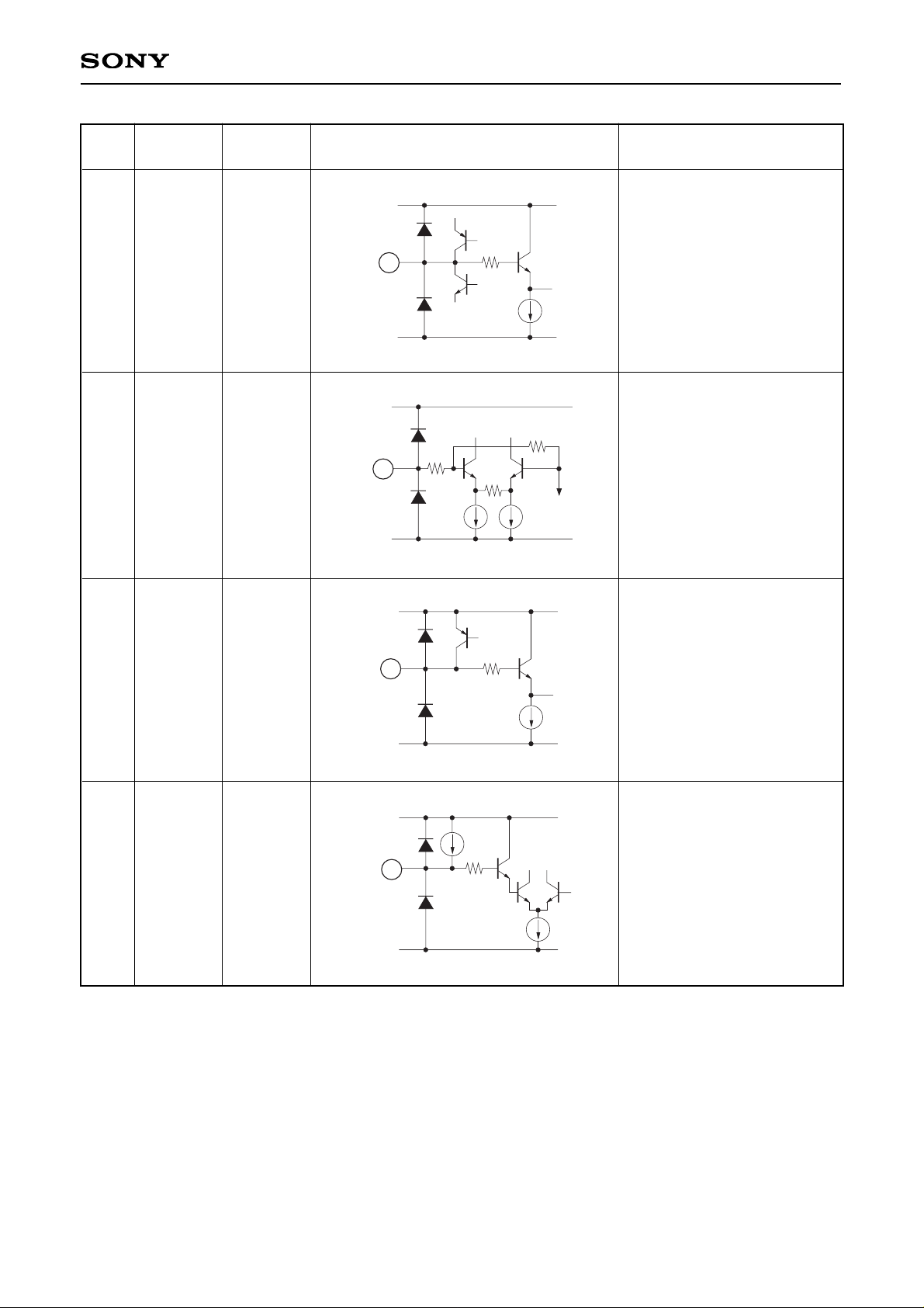
– 9 –
CXA2543R
61 Y IN
Y signal input.
The standard signal input level
is 0.5Vp-p (100% white level
from the sync tip).
Input at low impedance (75Ω
or less).
VCC1
GND1
70µA
1k
61
63 F0 ADJ
3.0V
Connect resistance of 15kΩ
between this pin and GND1 to
adjust the internal filters using
the outflow current value.
Connect to +4.5V power
supply when using Y/C or
Y/color difference input.
VCC1
GND1
15µA
1k
63
64 PWRST —
TG block system reset pin.
The system is reset when this
pin is connected to GND.
Connect a capacitor between
this pin and GND.
1k
VDD1
GND1
2µA
64
62 PIC
—
Adjusts frequency response of
luminance signal.
Increasing the voltage
emphasizes contours.
VCC1
GND1
30k
10k
50µA
20k
50µA
62
BIAS
3.1V
Pin
No.
Symbol Pin voltage Equivalent circuit Description
– 10 –
CXA2543R
Setting Conditions for Measuring Electrical Characteristics
Use the electrical characteristics measurement circuit on page 30 when measuring electrical characteristics.
Also, the TG (timing generator) block must be initialized by performing Settings 1 and 2 below.
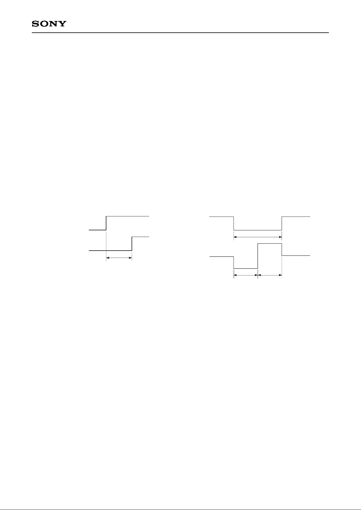
Setting 1. System reset
After turning on the power, set SW64 to ON and start up V64 from GND in order to activate the TG block
system reset. (See Fig. 1-1.)
The serial bus will be set to default values.
Setting 2. Horizontal AFC adjustment
Input SIG5 (VL = 0mV) to (A) and adjust V14 so that WL and WH of the TP12 output waveform are the
same. (See Fig. 1-2.)
Note) When measuring a band of 2MHz or more for Y signal frequency response or sharpness response
among the items being measured, the measurement must be made with sample-and-hold timing (serial
bus) set to through (sample-and- hold not performed).
VDD
V64 (PWRST)
T
R > 10µs
T
R
SIG5
TP12
WL = WH
WL
WH
WS
Fig. 1-1. System reset Fig. 1-2. Horizontal AFC adjustment
– 11 –
CXA2543R
Electrical Characteristics — DC Characteristics
Unless otherwise specified, Settings 1 and 2 and the following setting conditions are required.
VCC1 = 4.5V, VCC2 = 12.0V, VCC3 = 12.0V, GND1 = GND2 = GND3 = 0V, VDD1 = 3.0V, VSS1 = VSS2 = 0V, Ta = 25°C
SW54, SW62, SW64 = ON
SW6, SW7, SW8, SW59 = A
SW51, SW52 = B
V54 = 0V, V62 = 2.2V
Set the serial bus registers to the "Serial Bus Register Initial Settings". Unspecified the serial bus registers
should be set to default settings.
Input SIG4 to (A) and SIG2 (0dB) to (B).
Measure the I
CC1 current value.
COMP input mode
Input SIG4 to (A) and SIG2 (0dB) to (B).
Measure the I
CC1 current value.
Y/C input mode
Input SIG4 to (A), (D) and (E).
Measure the I
CC1 current value.
SW51, SW52 = A, SW59 = B
Y/color difference input mode
Input SIG4 to (A) and SIG2 (0dB) to (B).
Measure the I
CC2 current value.
PSIG load capacity CLP = 0pF
Input SIG4 to (A) and SIG2 (0dB) to (B).
Adjust PSIG-BRT of the serial bus and measure the
I
CC2 current value when TP39 output is set to 5Vp-p.
PSIG load capacity CLP = 10000pF
Input SIG4 to (A) and SIG2 (0dB) to (B).
Measure the I
DD current value.
DCX501 and LCX018 (4:3) mode
Input SIG4 to (A) and SIG2 (0dB) to (B).
Measure the I
DD current value.
LCX018 (16:9) mode
23
21
17
6
6
6
7.5
30
28
23
8
8.3
8
10
37
35
29
10
10.5
10
12.5
mA
mA
mA
mA
mA
mA
mA
I
CC11
I
CC12
I
CC13
I
CC2A
I
CC2B
I
DD1
I
DD2
Item
Power supply characteristics
Current
consumption
V
CC1
Current
consumption
V
CC2, 3
Current
consumption V
DD
Symbol Conditions Min. Typ. Max. Unit
– 12 –
CXA2543R
Digital block input pin
∗
1
0.3VDD
V
VIL
Digital block I/O characteristics
Low level input voltage
High level input voltage
Input current
CKI pin low input current
CKI pin high input current
High level output voltage
Output pins except
CKO and RPD
Low level output voltage
Output pins except
CKO and RPD
High level output voltage
CKO pin
Low level output voltage
CKO pin
High level output voltage
RPD pin
Low level output voltage
RPD pin
Output off leak current
RPD pin
Digital block input pin
∗
1
0.7VDD
V
VIH
Input pin with pull-up resistor
∗
2
VIN = VSS2
–145
–60
–24
µA
II1
VIN = VSS
–10
µA
II2
VIN = VDD1
10
µA
II3
IOH = –1mA
∗
3
2.8
V
VOH1
IOL = 1mA
∗
3
0.3
V
VOL1
IOH = –3mA
0.5V
DD
V
VOH2
IOL = 3mA
0.5V
DD
V
VOL2
∗1
Digital block input pins: SCLK, DATA, LOAD, VDIN, RGT, FLDIN, CKI
∗2
Input pins with pull-up resistors: SCLK, DATA, LOAD, VDIN, RGT, FLDIN
∗3
Output pins except CKO and RPD: XHST, HST, HCK1, HCK2, XPCG, PCG, HD, XVST, VST, VCK1, VCK2,
XEN, EN, VD
IOH = –0.5mA
V
DD – 1.2
V
VOH3
IOL = 0.7mA
1.0
V
VOL3
High impedance status
VOUT = V
SS or VOUT = VDD1
–40
40
µA
IOFF
Item Symbol Conditions Min. Typ. Max. Unit
– 13 –
CXA2543R
Electrical Characteristics — AC Characteristics
Unless otherwise specified, Settings 1 and 2 and the following setting conditions are required.
VCC1 = 4.5V, VCC2 = 12.0V, VCC3 = 12.0V, GND1 = GND2 = GND3 = 0V, VDD1 = 3.0V, VSS1 = VSS2 = 0V, Ta = 25°C
SW54, SW62, SW64 = ON
SW6, SW7, SW8 = A
SW51, SW52, SW59 = B
V54 = 0V, V62 = 2.2V
Set the serial bus registers to the "Serial Bus Register Initial Values". Unspecified serial bus registers should
be set to default settings.
Unless otherwise specified, measure the non-inverted outputs for TP41, TP44 and TP46.
Input SIG2 (0dB) to (A). Using a spectrum
analyzer, measure the input and the 3.58MHz or
4.43MHz component of TP44, and obtain
CRLEKY = 150mV × 10
∆CLK/20
using their
difference ∆CLK.
19
13
–9
5.0
2.5
3.0
5.0
22
17
–5
25
21
–1
dB
dB
dB
MHz
MHz
MHz
MHz
GV
GCNTTP
GCNTMN
FCYYC
FCYCMN
FCYCMP
Y signal block
Video maximum
gain
Contrast
characteristics TYP
Contrast
characteristics MIN
Y signal frequency
response 1
Y signal frequency
response 2
10 14
–2 0
6 9
–4 –2
dB
dB
dB
dB
GSHP1X
FCL
GSHP1N
GSHP2X
GSHP2N
Picture quality
adjustment
variable amount 1
(Y/C input)
Picture quality
adjustment
variable amount 2
(composite input)
CRLEKY 30 mV
Carrier leak
(residual carrier)
Y/C input
Composite input
(NTSC)
Composite input
(PAL)
TDYYC
TDYCMN
TDYCMP
250
570
570
350
670
670
450
770
770
ns
ns
ns
Y signal I/O delay
time
Y/C input
Composite input
(NTSC)
Composite input
(PAL)
Input SIG9 (VL = 150mV) to
(A). Measure the delay time
from the 2T pulse peak of
the input signal to the peak
of the non-inverted output at
TP44.
Input SIG4 to (A) and measure the ratio between the output
amplitude (white-black) and input amplitude at TP44.
Input SIG4 to (A) and measure the ratio between the output
amplitude (white-black) and input amplitude at TP44.
Input SIG4 to (A) and measure the ratio between the output
amplitude (white-black) and input amplitude at TP44.
Assume the output amplitude at
TP44 when SIG7 (0dB, no burst,
100kHz) is input to (A) as 0dB.
Vary the frequency of the input
signal to obtain the frequency with
an output amplitude of –3dB.
V62 = 1.5V
Assume the output amplitude at TP44 when SIG7
(0dB, no burst, 100kHz) is input to (A) as 0dB.
Vary the frequency of the input signal to obtain the
frequency with an output amplitude of –3dB.
V62 = 1.5V, Load 500pF
Assume the output amplitude at TP44 when SIG7
(100kHz) is input to (A) as 0dB. Set SIG7 to 2.5MHz
and measure GSHP1X and GSHP1N as the
amounts by which the output amplitude at TP44
changes when V62 = 4V and 0V, respectively.
Assume the output amplitude at TP44 when SIG7
(100kHz) is input to (A) as 0dB. Set SIG7 to 2.0MHz
and measure GSHP2X and GSHP2N as the
amounts by which the output amplitude at TP44
changes when V62 = 4V and 0V, respectively.
Item Symbol Conditions Min. Typ. Max. Unit
– 14 –
CXA2543R
Input SIG5 (VL = 150mV) to (A) and
SIG2 (level variable, 3.58MHz
burst/chroma phase = 180°, or 4.43MHz
burst/chroma phase = ±135°) to (B), and
measure the output amplitude at TP44.
Gradually reduce the SIG3 amplitude
level and measure the level at which the
killer operation is activated.
SW59 = A
–3
0
3 dB
–3 0 3
dB
–4
–1
2
dB
–4
±500
Hz
±500 Hz
4 6 dB
–25
–15
dB
–37 –31 dB
–34
–28
dB
–1
2
dB
ACC1
ACC2
FAPCN
FAPCP
GCOLMX
GCOLMN
ACKN
ACKP
Chroma signal block
ACC amplitude
characteristics 1
ACC amplitude
characteristics 2
APC pull-in range
Color adjustment
characteristics
MAX
Color adjustment
characteristics
MIN
–30 –40 deg
30 60 deg
HUEMX
HUEMN
HUE adjustment
range
MAX
HUE adjustment
range
MIN
Killer operation
input level
NTSC
PAL
NTSC
PAL
NTSC
PAL
NTSC
PAL
Input SIG5 (VL = 150mV) to (A) and
SIG2 (0dB/+6dB/–20dB, 3.58MHz
burst/chroma phase = 180°, or 4.43MHz
burst/chroma phase = ±135°) to (B).
Measure the output amplitude at TP53,
assuming the output corresponding to
0dB, +6dB and –20dB as V0, V1 and V2,
respectively.
ACC1 = 20 log (V1/V0)
ACC2 = 20 log (V2/V0)
SW59 = A
Input SIG5 (VL = 150mV) to (A) and
SIG2 (0dB, 3.58MHz burst/chroma
phase = 180°, or 4.43MHz burst/chroma
phase = ±135°) to (B). Changing the
SIG2 burst frequency, measure the
frequency f1 at which the TP44 output
appears (the killer mode is canceled).
NTSC: FAPCN = f1 – 3579545Hz
PAL: FAPCP = f1 – 4433619Hz
SW59 = A
Input SIG5 (VL = 150mV) to (A) and SIG2 (0dB,
3.58MHz burst/chroma phase = 180°) to (B).
Assume the chroma output amplitude when serial
bus register COLOR = 80H, 0FFH and 0H as V0,
V1 and V2, respectively.
GCOLMX = 20 log (V1/V0)
GCOLMN = 20 log (V2/V0)
SW59 = A
Input SIG5 (VL = 150mV) to (A) and SIG2 (0dB,
burst/chroma phase variable) to (B). Assume the
phase at which the output amplitude at TP44
reaches a minimum when serial bus register HUE
= 80H, 0FFH and 0H as θ0, θ1 and θ2,
respectively.
HUEMX = θ1 – θ0
HUEMN = θ2 – θ0
SW59 = A
Item Symbol Conditions Min. Typ. Max. Unit
– 15 –
CXA2543R
Demodulation
output amplitude
ratio (NTSC)
Demodulation
output amplitude
ratio (PAL)
Demodulation
output phase
difference (PAL)
Color difference
balance
θRBN
VGBN
VRBN
θGBN
VRBP
VGBP
99
0.25
0.53
230
109
0.32
0.63
242
119
0.39
0.73
254
deg
0.33
0.65
0.40
0.75
0.47
0.85
deg
θRBP
θGBP
80
232
90
244
100
256
deg
deg
GEXCMX
4 6 dB
GEXCMN
Color difference
input color
adjustment
characteristics
MAX
Color difference
input color
adjustment
characteristics
MIN
Color difference
input balance
adjustment R
Color difference
input balance
adjustment B
–20 –15
dB
VEXCBL 0.8 1.0 1.2
GEXRMX 2 3 dB
GEXRMN
–3
–2 dB
GEXBMX
–3
–2 dB
GEXBMN
2
3
dB
Input SIG5 (VL = 150mV) to (A) and SIG2 (0dB,
3.58MHz) to (B) and change the chroma phase.
Assume the maximum amplitude at TP41 as VB,
the maximum amplitude at TP44 as VG, and the
maximum amplitude at TP46 as VR.
VRBN = VR/VB, VGBN = VG/VB
SW59 = A
Input SIG5 (VL = 150mV) to (A) and SIG2 (0dB,
3.58MHz) to (B) and change the chroma phase.
Assume the phase at which the amplitude at
TP41, TP44 and TP46 reaches a maximum as
θB, θG and θR, respectively.
θRBN = θR – θB, θGBN = θG – θB
SW59 = A
Input SIG5 (VL = 150mV) to (A) and SIG2 (0dB,
4.43MHz) to (B) and change the chroma phase.
Assume the maximum amplitude at TP41 as VB,
the maximum amplitude at TP44 as VG, and the
maximum amplitude at TP46 as VR.
VRBP = VR/VB, VGBP = VG/VB
SW59 = A
Input SIG5 (VL = 150mV) to (A) and SIG2 (0dB,
4.43MHz) to (B) and change the chroma phase.
Assume the phase at which the amplitude at
TP41, TP44 and TP46 reaches a maximum as
θB, θG and θR, respectively.
θRBP = θR – θB, θGBP = θG – θB
SW59 = A
Input SIG5 (VL = 150mV) to (A) and SIG1 (0dB,
100kHz, no burst) to (D). Assume the output
amplitude at TP41 (100kHz) when serial bus
register COLOR = 80H as VC0, when COLOR =
0H as VC2, and when SIG1 is set to -10dB and
COLOR = 0FFH as VC1.
GEXCMX = 20 log (VC1/VC0) + 10
GEXCMN = 20 log (VC2/VC0)
SW51, SW52 = A
Input SIG5 (VL = 150mV) to (A) and SIG1 (0dB,
100kHz, no burst) to (D) and (E). Assume the
output amplitude at TP41 (100kHz) as VB and
the output amplitude at TP46 (100kHz) as VR.
VEXCBL = VR/VB
SW51, SW52 = A
Input SIG5 (VL = 150mV) to (A) and SIG1 (–6dB,
100kHz, no burst) to (D) and (E). Assume the
output amplitude at TP46 (100kHz) and TP41
(100kHz) when serial bus register HUE = 80H as
VR0 and VB0, respectively, when HUE = 0FFH
as VR1 and VB1, respectively, and when HUE =
0H as VR2 and VB2, respectively.
GEXRMX = 20 log (VR1/VR0)
GEXRMN = 20 log (VR2/VR0)
GEXBMX = 20 log (VB1/VB0)
GEXBMN = 20 log (VB2/VB0)
SW51, SW52 = A
Item Symbol Conditions Min. Typ. Max. Unit
Demodulation
output phase
difference (NTSC)
– 16 –
CXA2543R
VEXGBN 0.22 0.25 0.28
0.47 0.53 0.58
VEXGRN
5.85
9.0
9.0
6.00
0
6.15
100
5.2
4.0
V
mV
Vp-p
Vp-p
Vp-p
Vp-p
G-Y matrix
characteristics
(NTSC)
Input SIG5 (VL = 150mV) to (A) and SIG1 (0dB,
100kHz, no burst) to (D). Assume the output
amplitude at TP41 (100kHz) as VEXB and the
output amplitude at TP44 (100kHz) as VEXBG.
VEXGBN = VEXBG/VEXB
SW51, SW52 = A
Input SIG5 (VL = 150mV) to (A) and SIG1 (0dB,
100kHz, no burst) to (E). Assume the output
amplitude at TP46 (100kHz) as VEXR and the
output amplitude at TP44 (100kHz) as VEXRG.
VEXGRN = VEXRG/VEXR
SW51, SW52 = A
VEXGBP 0.16 0.19 0.22
0.48 0.53 0.58
VEXGRP
G-Y matrix
characteristics
(PAL)
Input SIG5 (VL = 150mV) to (A) and SIG1 (0dB,
100kHz, no burst) to (D). Assume the output
amplitude at TP41 (100kHz) as VEXB and the
output amplitude at TP44 (100kHz) as VEXBG.
VEXGBP = VEXBG/VEXB
SW51, SW52 = A
Input SIG5 (VL = 150mV) to (A) and SIG1 (0dB,
100kHz, no burst) to (E). Assume the output
amplitude at TP46 (100kHz) as VEXR and the
output amplitude at TP44 (100kHz) as VEXRG.
VEXGRP = VEXRG/VEXR
SW51, SW52 = A
VOUT
∆VOUT
VLIMMX
VLIMMN
BRTMX
BRTMN
Input SIG5 (VL = 0mV) to (A). Adjust serial bus
register BRIGHT so that the output (black-black)
at TP44 is 9Vp-p and measure the DC voltage at
TP39, TP41, TP44 and TP46.
Input SIG5 (VL = 0mV) to (A). Adjust serial bus
register BRIGHT so that the output (black-black) at
TP44 is 9Vp-p, measure the DC voltage at TP39,
TP41, TP44 and TP46, and obtain the maximum
difference between each of these values.
Input SIG3 to (A). Vary V54 and measure the maximum
value VLIMMX and minimum value VLIMMN of the
voltage range (black-black) over which the black limiter
operates for the TP39, TP41, TP44 and TP46 outputs.
Assume the value whenV54 = 0V as VLIMMX, and
when V54 = 4.5V as VLIMMN.
Input SIG5 (VL = 0mV) to (A) and measure the
output (black-black) at TP41, TP44 and TP46
when serial bus register BRIGHT = 0H.
Input SIG5 (VL = 0mV) to (A) and measure the
output (black-black) at TP41, TP44 and TP46
when serial bus register BRIGHT = 0FFH.
RGB signal output block
RGB signal and
PSIG output DC
voltage
RGB signal and
PSIG output DC
voltage difference
RGB and PSIG
output limiter
operation voltage
Amount of change
in brightness
Item Symbol Conditions Min. Typ. Max. Unit
– 17 –
CXA2543R
1.5
Vp-p
9.0
Vp-p
±
1.5
±2.0
V
PSIGMX
PSIGMN
Input SIG5 (VL = 0mV) to (A) and measure the
output (black-black) at TP39 when serial bus
register PSIG-BRT = 0H.
Input SIG5 (VL = 0mV) to (A) and measure the
output (black-black) at TP39 when serial bus
register PSIG-BRT = 0FFH.
Amount of change
in PSIG
SBBRT
Input SIG5 (VL = 0mV) to (A) and measure the difference
between the outputs (black-black) at TP41 and TP46 and
the output (black-black) at TP44 when serial bus registers
R-BRT = B-BRT = 0H and when R-BRT = B-BRT = 0FFH.
Amount of change
in sub-brightness
–0.5
0
0.5
dB
∆GRGB
Input SIG4 to (A) and obtain the level difference between
the maximum and minimum non-inverted output
amplitudes (white-black) at TP41, TP44 and TP46.
Difference in gain
between RGB
output signals
–0.5
0
0.5
dB
∆GINV
Input SIG4 to (A) and obtain the level difference between
the non-inverted output amplitudes (white-black) and the
inverted output amplitudes at TP41, TP44 and TP46.
Difference in RGB
output inverted/noninverted gain
300
mV
∆VBL
Input SIG4 to (A) and obtain the level difference between
the maximum and minimum black levels of both the inverted
and non-inverted outputs at TP41, TP44 and TP46.
Input SIG8 to (A). Adjust the non-inverted output
black level at TP44 to 6.0
-
4.5V with serial bus
register BRIGHT and the non-inverted output
amplitude (white-black) at TP44 to 3.5V with
serial bus register CONTRAST. Measure VG1,
VG2 and VG3.
Gγ1 = 20 log (VG1/0.0357)
Gγ2 = 20 log (VG2/0.0357)
Gγ3 = 20 log (VG3/0.0357)
(See Fig. 5 for definitions of VG1, VG2 and VG3.)
Input SIG8 to (A) and adjust serial bus register
BRIGHT so that the output at TP44 is 9Vp-p
(black-black). Read the point where the gain of
the non-inverted output at TP44 changes when
serial bus register γ1 = 0H and 0FFH from the
input signal IRE level.
Vγ1MN when γ1 = 0H, and Vγ1MX when γ1 =
0FFH.
Input SIG8 to (A) and adjust serial bus register
BRIGHT so that the output at TP44 is 9Vp-p
(black-black). Read the point where the gain of
the non-inverted output at TP44 changes when
serial bus register γ2 = 0H and 0FFH from the
input signal IRE level.
Vγ2MN when γ2 = 0H, and Vγ2MX when γ2 =
0FFH.
Difference in black
level potential between
RGB output signals
γ gain
γ1 adjustment
variable range
γ2 adjustment
variable range
Gγ1
Gγ2
Gγ3
23.0
26.0 29.0
dB
12.0
15.0 18.0
dB
18.0
21.0 25.0
dB
Vγ1MN
Vγ1MX
Vγ2MN
Vγ2MX
0 IRE
100 IRE
100 IRE
0 IRE
Input SIG4 to (A) and adjust serial bus register
PSIG-BRT so that the output at TP39 is 9Vp-p
(black-black). Measure the time it takes to change
to an amplitude of 9Vp-p.
tPSIGH: rising edge, tPSIGL: falling edge
PSIG transition
time
tPSIGH
tPSIGL
1.5 3.0 µs
1.5 3.0
µs
Input SIG5 (VL = 350mV) to (A) and measure the voltage (whitewhite) at which the white limiter activates for inverted output and
non-inverted output at TP41, TP44 and TP46, respectively.
RGB output white
limiter operation
voltage
VWLIM
1.3 1.5 1.7
V
Input SIG5 (VL = 0mV) to (A) and adjust V54 so that
the output at TP44 is 9Vp-p (black-black). Measure the
DC voltage at TP41, TP44 and TP46 and obtain the
difference versus the RGB output voltage VOUT.
Black limiter DC
voltage difference
∆VBLIM
0 100 mV
Item Symbol Conditions Min. Typ. Max. Unit
– 18 –
CXA2543R
TDSYL
TDSYH
HPLLN
HPLLP
430
630 830 ns
4.7
5.0 5.3 µs
±500
Hz
±500
Hz
NTSC
PAL
0 100 mV
ATBPF
ATRAPN
ATRAPP
DEMLPF
WSSEP
VSSEP
–16 –10 dB
–16 –10 dB
–7 –2 dB
–8 –3 dB
–40
–30 dB
–40 –30 dB
0.8
1.0
1.3 MHz
2.0 µs
40 60 mV
NTSC 1.5MHz
PAL 2.0MHz
NTSC 5.5MHz
PAL 6.8MHz
NTSC
PAL
Amount of BPF
attenuation
Amount of TRAP
attenuation
R-Y, B-Y and LPF
characteristics
Input sync signal
width sensitivity
Sync separation
input sensitivity
Sync separation
output delay time
Horizontal pull-in
range
Sync separation, TG block
Filter characteristics
Assume the chroma amplitude at TP53
when SIG5 (VL = 0mV) is input to (A)
and SIG1 (0dB at input center frequency
(3.58Hz or 4.43Hz)) is input to (B) as
0dB. Obtain the amount by which the
output at TP53 is attenuated when the
frequencies noted on the right are input.
SW59 = A
Input SIG2 (0dB, 3.58Hz and 4.43Hz) to (A)
and measure the output at TP44. Assume
the amplitude at TP44 during Y/C input
mode as 0dB, and obtain the amount of
attenuation during COMP input mode.
Assume the amplitude of the 100kHz component of the output at
TP44 when SIG5 (VL = 150mV) is input to (A) and SIG1 (0dB,
3.58Hz + 100kHz) is input to (B) as 0dB. Obtain the frequency
which attenuates the beat component of the output by 3dB when
the SIG1 frequency is increased with respect to 3.58MHz.
SW59 = A
Input SIG5 (VL = 0mV, VS = 143mV, WS variable) to (A) and
confirm that it is synchronized with the HD output at TP23.
Gradually narrow the WS of SIG5 from 4.7µs and obtain the WS
at which synchronization with the HD output at TP23 is lost.
Input SIG5 (VL = 0mV, WS = 4.7µs, VS = variable) to (A) and
confirm that it is synchronized with the HD output at TP23.
Gradually reduce the VS of SIG5 from 143mV and obtain the VS
at which synchronization with the HD output at TP23 is lost.
Input SIG5 (VL = 0mV, WS = 4.7µs, VS = 143mV) to (A) and
measure the delay time with the RPD output at TP12. TDSYL is
from the falling edge of the input HSYNC to the falling edge of the
RPD output at TP12, and TDSYH is from the falling edge of the
input HSYNC to the rising edge of the RPD output at TP12.
Input SIG5 (VL = 0mV, WS = 4.7µs, VS = 143mV,
horizontal frequency variable) to (A) and confirm that it
is synchronized with the HD output at TP23. Obtain the
frequency f
H at which the input and output are
synchronized by changing the horizontal frequency of
SIG5 from the non-synchronized condition.
HPLLN = f
H – 15734
HPLLP = f
H – 15625
∆VWLIM
White limiter DC
voltage difference
Input SIG5 (VL = 350mV) to (A). Measure the DC
voltage at TP41, TP44 and TP46 and obtain the
difference versus the RGB output voltage VOUT.
3.0
V
VDROFF
RGB output range
when FRP polarity
reverse is stopped
Input SIG8 to (A). Assume the black limiter level of
the output at TP41, TP44 and TP46 when serial bus
register BRIGHT = 0H as VDRB and the white
limiter level when BRIGHT = OFFH as VDRW.
VDROFF = VDRW – VDRB
Item Symbol Conditions Min. Typ. Max. Unit
– 19 –
CXA2543R
tTLH
tTHL
∆T
DTYHC
VTEXTB
VTEXTW
TDEXTH
TDEXTL
EXTBK
EXTWT
30
ns
30
ns
10
ns
47 50 53
%
0.8 1.0 1.2
V
1.8
2.0 2.2
V
50 100
150
ns
50 100 150
ns
0
V
3.5
V
180
ns
Output transition
time (P12
∗
3
pin)
Cross-point time
difference
HCK duty
Input SIG5 (VL = 0mV) to (A).
Measure the transition time for each output.
Load = 30pF
(See Fig. 3.)
Input SIG5 (VL = 0mV) to (A).
Measure HCK1/HCK2.
Load = 30pF
(See Fig. 4.)
Input SIG5 (VL = 0mV) to (A).
Measure the HCK1/HCK2 duty.
Load = 30pF
LOAD setup time, activated by the rising edge of
SCLK. (See Fig. 6.)
DATA setup time, activated by the rising edge of
SCLK. (See Fig. 6.)
LOAD hold time, activated by the rising edge of
SCLK. (See Fig. 6.)
DATA hold time, activated by the rising edge of
SCLK. (See Fig. 6.)
SCLK pulse width. (See Fig. 6.)
SCLK pulse width. (See Fig. 6.)
LOAD pulse width. (See Fig. 6.)
150
150
150
150
1
160
160
ns
ns
ns
ns
ns
ns
µs
ts0
ts1
th0
th1
tw1L
tw1H
tw2
Serial transfer block
Data setup time
Data hold time
Minimum pulse
width
Input SIG5 (VL = 0mV) to (A) and SIG6 (VL variable) to (C).
Raise the SIG6 amplitude (VL) from 0V and assume the voltage
where the outputs at TP41, TP44 and TP46 go to black level as
VTEXTB. Then raise the amplitude further and assume the
voltage where these outputs go to white level as VTEXTW.
SW6, SW7, SW8 = B
Input SIG5 (VL = 0mV) to (A) and SIG6 (VL = 3V)
to (C). Measure the rise delay time TD1EXT and
the fall delay time TD2EXT of the outputs at
TP41, TP44 and TP46.
(See Fig. 2.)
SW6, SW7, SW8 = B
Input SIG5 (VL = 0mV) to (A) and SIG6 (VL = 1.7V)
to (C). Measure the difference from the black level
of the outputs at TP41, TP44 and TP46.
SW6, SW7, SW8 = B
Input SIG5 (VL = 0mV) to (A) and SIG6 (VL = 2.7V)
to (C). Measure the difference from the black level
of the outputs at TP41, TP44 and TP46.
SW6, SW7, SW8 = B
TEXTMIN
Input SIG5 (VL = 0mV) to (A) and SIG6 (VL = 2.7V) to (C).
Measure the minimum pulse width at which each of the
outputs at TP41, TP44 and TP46 reach the white limiter.
SW6, SW7, SW8 = B
External I/O characteristics
External RGB input
threshold voltage
Propagation delay
time between
external RGB input
and output
Output blanking
level during
external RGB input
Output white level
during external
RGB input
Minimum pulse
width during
external RGB input
Item Symbol Conditions Min. Typ. Max. Unit
– 20 –
CXA2543R
Setting 2
Power supply characteristics
Digital block I/O characteristics
Description of Electrical Characteristics Measurement Methods
Serial Bus Register Initial Values
Item Symbol
Serial bus
Mode settings
Input System Aspect S/H HUE COLOR BRIGHT
CONTRAST
R-BRT B-BRT
γ1 γ2
DAC settings
Low level input voltage
High level input voltage
Input current
CKI pin low input current
CKI pin high input current
High level output voltage
Low level output voltage
High level output voltage
Low level output voltage
High level output voltage
Low level output voltage
Output off leak current
ICC11
ICC12
ICC13
ICC2A
ICC2B
IDD1
IDD2
VIL
VIH
II1
II2
II3
VOH1
VOL1
VOH2
VOL2
VOH3
VOL3
IOFF
COMP
COMP
Y/C
Y/color
difference
COMP
COMP
COMP
COMP
COMP
COMP
COMP
COMP
COMP
COMP
COMP
COMP
COMP
COMP
COMP
COMP
NTSC
NTSC
NTSC
NTSC
NTSC
NTSC
NTSC
NTSC
NTSC
NTSC
NTSC
NTSC
NTSC
NTSC
NTSC
NTSC
NTSC
NTSC
NTSC
NTSC
Panel
—
—
—
—
—
—
—
LCX018
—
—
—
—
—
—
—
—
—
—
—
—
—
—
—
—
—
—
4:3
16:9
—
—
—
—
—
—
—
—
—
—
—
—
SHS1
SHS1
SHS1
SHS1
SHS1
SHS1
SHS1
SHS1
SHS1
SHS1
SHS1
SHS1
SHS1
SHS1
SHS1
SHS1
SHS1
SHS1
SHS1
SHS1
80H
80H
80H
80H
80H
80H
80H
80H
80H
80H
80H
80H
80H
80H
80H
80H
80H
80H
80H
80H
80H
80H
80H
80H
80H
80H
80H
80H
80H
80H
80H
80H
80H
80H
80H
80H
80H
80H
80H
80H
80H
80H
80H
80H
80H
80H
80H
80H
80H
80H
80H
80H
80H
80H
80H
80H
80H
80H
80H
80H
80H
80H
80H
80H
80H
80H
80H
80H
80H
80H
80H
80H
80H
80H
80H
80H
80H
80H
80H
80H
80H
80H
80H
80H
80H
80H
80H
80H
80H
80H
80H
80H
80H
80H
80H
80H
80H
80H
80H
80H
80H
80H
80H
80H
80H
80H
80H
80H
80H
80H
80H
80H
80H
80H
80H
80H
80H
80H
80H
80H
0H
0H
0H
0H
0H
0H
0H
0H
0H
0H
0H
0H
0H
0H
0H
0H
0H
0H
0H
0H
0H
0H
0H
0H
0H
0H
0H
0H
0H
0H
0H
0H
0H
0H
0H
0H
0H
0H
0H
0H
PSIG-BRT
80H
80H
80H
80H
80H
78H
80H
80H
80H
80H
80H
80H
80H
80H
80H
80H
80H
80H
80H
80H
(–: don't care, ADJ: adjustment, SET: setting)
Horizontal AFC
adjustment
Current
consumption V
CC1
Current
consumption V
CC2,3
Current
consumption V
DD
– 21 –
CXA2543R
Y signal block
Item Symbol
Serial bus
Mode settings
Input System Aspect S/H HUE COLOR BRIGHT
CONTRAST
R-BRT B-BRT
γ1 γ2
DAC settings
Video maximum gain
Contrast
characteristics TYP
Contrast
characteristics MIN
Y signal frequency
response 1
Y signal frequency
response 2
Picture quality
adjustment variable
amount 1
Picture quality
adjustment variable
amount 2
Carrier leak
Y signal I/O delay
time
GV
GCNTTP
GCNTMN
FCYYC
FCYCMN
FCYCMP
FCL
GSHP1X
GSHP1N
GSHP2X
GSHP2N
CRLEKY
TDYYC
TDYCMN
TDYCMP
COMP
COMP
COMP
Y/C
COMP
COMP
Y/C
Y/C
Y/C
COMP
COMP
COMP
Y/C
COMP
COMP
NTSC
NTSC
NTSC
NTSC
NTSC
PAL
NTSC
NTSC
NTSC
NTSC
NTSC
—
—
NTSC
PAL
Panel
—
—
—
—
—
—
—
—
—
—
—
—
—
—
—
—
—
—
—
—
—
—
—
—
—
—
—
—
—
—
Through
Through
Through
Through
Through
Through
Through
Through
Through
Through
Through
Through
Through
Through
Through
80H
80H
80H
80H
80H
80H
80H
80H
80H
80H
80H
80H
80H
80H
80H
80H
80H
80H
80H
80H
80H
80H
80H
80H
80H
80H
80H
80H
80H
80H
0A0H
0A0H
0A0H
0A0H
0A0H
0A0H
0A0H
60H
60H
60H
60H
60H
96H
96H
96H
0FFH
80H
0H
80H
80H
80H
80H
80H
80H
80H
80H
80H
80H
80H
80H
80H
80H
80H
80H
80H
80H
80H
80H
80H
80H
80H
80H
80H
80H
80H
80H
80H
80H
80H
80H
80H
80H
80H
80H
80H
80H
80H
80H
80H
80H
0H
0H
0H
0H
0H
0H
0H
0H
0H
0H
0H
0H
0H
0H
0H
0H
0H
0H
0H
0H
0H
0H
0H
0H
0H
0H
0H
0H
0H
0H
PSIG-BRT
80H
80H
80H
80H
80H
80H
80H
80H
80H
80H
80H
80H
80H
80H
80H
(–: don't care, ADJ: adjustment, SET: setting)
– 22 –
CXA2543R
Chroma signal block
Item
Symbol
Serial bus
Mode settings
Input System Aspect S/H HUE COLOR BRIGHT
CONTRAST
R-BRT B-BRT
γ1 γ2
DAC settings
ACC amplitude
characteristics 1
ACC amplitude
characteristics 2
APC pull-in range
Color adjustment
characteristics MAX
Color adjustment
characteristics MIN
HUE adjustment
range MAX
HUE adjustment
range MIN
Killer operation
input level
Demodulation output
amplitude ratio NTSC
Demodulation output
phase difference NTSC
Demodulation output
amplitude ratio PAL
Demodulation output
phase difference PAL
ACC1
ACC1
ACC2
ACC2
FAPCN
FAPCP
GCOLMX
GCOLMN
HUEMX
HUEMN
ACKN
ACKP
VRBN
VGBN
θRBN
θGBN
VRBP
VGBP
θRBP
θGBP
COMP
COMP
COMP
COMP
COMP
COMP
COMP
COMP
COMP
COMP
COMP
COMP
COMP
COMP
COMP
COMP
COMP
COMP
COMP
COMP
NTSC
PAL
NTSC
PAL
NTSC
PAL
NTSC
NTSC
NTSC
NTSC
NTSC
PAL
NTSC
NTSC
NTSC
NTSC
PAL
PAL
PAL
PAL
Panel
—
—
—
—
—
—
—
—
—
—
—
—
—
—
—
—
—
—
—
—
—
—
—
—
—
—
—
—
—
—
—
—
—
—
—
—
—
—
—
—
Through
Through
Through
Through
Through
Through
Through
Through
Through
Through
Through
Through
Through
Through
Through
Through
Through
Through
Through
Through
80H
80H
80H
80H
80H
80H
80H
80H
0FFH
0H
80H
80H
80H
80H
80H
80H
80H
80H
80H
80H
80H
80H
80H
80H
80H
80H
0FFH
0H
80H
80H
80H
80H
80H
80H
80H
80H
80H
80H
80H
80H
96H
96H
96H
96H
96H
96H
96H
96H
96H
96H
60H
60H
60H
60H
60H
60H
60H
60H
60H
60H
80H
80H
80H
80H
80H
80H
80H
80H
80H
80H
80H
80H
80H
80H
80H
80H
80H
80H
80H
80H
80H
80H
80H
80H
80H
80H
80H
80H
80H
80H
80H
80H
80H
80H
80H
80H
80H
80H
80H
80H
80H
80H
80H
80H
80H
80H
80H
80H
80H
80H
80H
80H
80H
80H
80H
80H
80H
80H
80H
80H
0H
0H
0H
0H
0H
0H
0H
0H
0H
0H
0H
0H
0H
0H
0H
0H
0H
0H
0H
0H
0H
0H
0H
0H
0H
0H
0H
0H
0H
0H
0H
0H
0H
0H
0H
0H
0H
0H
0H
0H
PSIG-BRT
80H
80H
80H
80H
80H
80H
80H
80H
80H
80H
80H
80H
80H
80H
80H
80H
80H
80H
80H
80H
(–: don't care, ADJ: adjustment, SET: setting)
– 23 –
CXA2543R
Chroma signal block
RGB signal output block
Item Symbol
Serial bus
Mode settings
Input System Aspect S/H HUE COLOR BRIGHT
CONTRAST
R-BRT B-BRT
γ1 γ2
DAC settings
Color difference input
color adjustment
characteristics MAX
Color difference input
color adjustment
characteristics MIN
Color difference balance
Color difference input
balance adjustment R
Color difference input
balance adjustment B
G-Y matrix
characteristics NTSC
G-Y matrix
characteristics PAL
RGB signal and PSIG
output DC voltage
RGB signal and PSIG output
DC voltage difference
RGB and PSIG output
limiter operation voltage
Amount of change in
brightness
Amount of change in
PSIG
GEXCMX
GEXCMN
VEXCBL
GEXRMX
GEXRMN
GEXBMX
GEXBMN
VEXGBN
VEXGRN
VEXGBP
VEXGRP
VOUT
∆VOUT
VLIMMX
VLIMMN
BRTMX
BRTMN
PSIGMX
PSIGMN
Y/color
difference
Y/color
difference
Y/color
difference
Y/color
difference
Y/color
difference
Y/color
difference
Y/color
difference
Y/color
difference
Y/color
difference
Y/color
difference
Y/color
difference
—
—
—
—
—
—
—
—
—
—
—
—
—
—
—
NTSC
NTSC
PAL
PAL
—
—
—
—
—
—
—
—
Panel
—
—
—
—
—
—
—
—
—
—
—
—
—
—
—
—
—
—
—
—
—
—
—
—
—
—
—
—
—
—
—
—
—
—
—
—
—
—
Through
Through
Through
Through
Through
Through
Through
Through
Through
Through
Through
Through
Through
Through
Through
Through
Through
Through
Through
80H
80H
80H
0FFH0H0FFH
0H
80H
80H
80H
80H
80H
80H
80H
80H
80H
80H
80H
80H
0FFH
0H
80H
80H
80H
80H
80H
80H
80H
80H
80H
80H
80H
80H
80H
80H
80H
80H
80H
96H
96H
96H
96H
96H
96H
96H
96H
96H
96H
96H
ADJ
ADJ
0H
0H
0H
0FFH
80H
80H
80H
80H
80H
80H
80H
80H
80H
80H
80H
80H
80H
80H
80H
80H
80H
80H
80H
80H
80H
80H
80H
80H
80H
80H
80H
80H
80H
80H
80H
80H
80H
80H
80H
80H
80H
80H
80H
80H
80H
80H
80H
80H
80H
80H
80H
80H
80H
80H
80H
80H
80H
80H
80H
80H
80H
80H
80H
0H
0H
0H
0H
0H
0H
0H
0H
0H
0H
0H
0H
0H
0H
0H
0H
0H
0H
0H
0H
0H
0H
0H
0H
0H
0H
0H
0H
0H
0H
0H
0H
0H
0H
0H
0H
0H
0H
PSIG-BRT
80H
80H
80H
80H
80H
80H
80H
80H
80H
80H
80H
64H
64H
0FFH
0FFH
0FFH
0FFH
0FFH
0H
(–: don't care, ADJ: adjustment, SET: setting)
– 24 –
CXA2543R
RGB signal output block
Item Symbol
Serial bus
Mode settings
Input System Aspect S/H HUE COLOR BRIGHT
CONTRAST
R-BRT B-BRT
γ1 γ2
DAC settings
Amount of change in
sub-brightness
Difference in gain between
RGB output signals
Difference in RGB output
inverted/non-inverted gain
Difference in black
level potential between
RGB output signals
γ gain
γ1 adjustment
variable range
γ2 adjustment
variable range
PSIG transition time
RGB output white limiter
operation voltage
Black limiter DC
voltage difference
White limiter DC
voltage difference
RGB output range
when FRP polarity
reverse is stopped
SBBRT
∆GRGB
∆GINV
∆VBL
Gγ1
Gγ2
Gγ3
Vγ1MN
Vγ1MX
Vγ2MN
Vγ2MX
tPSIGH
tPSIGL
VWLIM
∆VBLIM
∆
VWLIM
VDROFF
—
—
—
—
—
—
—
—
—
—
—
—
—
—
—
—
—
—
—
—
—
—
—
—
—
—
—
—
—
—
—
—
—
—
Panel
—
—
—
—
—
—
—
—
—
—
—
—
—
—
—
—
—
—
—
—
—
—
—
—
—
—
—
—
—
—
—
—
—
—
Through
Through
Through
Through
Through
Through
Through
Through
Through
Through
Through
Through
Through
Through
Through
Through
Through
80H
80H
80H
80H
80H
80H
80H
80H
80H
80H
80H
80H
80H
80H
80H
80H
80H
80H
80H
80H
80H
80H
80H
80H
80H
80H
80H
80H
80H
80H
80H
80H
80H
80H
0B4H
80H
80H
80H
ADJ
ADJ
ADJ
ADJ
ADJ
ADJ
ADJ
60H
60H
0B4H
0H
0B4H
SET
80H
80H
80H
80H
ADJ
ADJ
ADJ
46H
46H
46H
46H
80H
80H
0FFH
80H
0FFH
80H
SET
80H
80H
80H
80H
80H
80H
80H
80H
80H
80H
80H
80H
80H
80H
80H
80H
SET
80H
80H
80H
80H
80H
80H
80H
80H
80H
80H
80H
80H
80H
80H
80H
80H
0H
0H
0H
0H
78H
78H
78H
0H
0FFH
0H
0H
0H
0H
0H
0H
0H
0H
0H
0H
0H
0H
0D7H
0D7H
0D7H
0H
0H
0H
0FFH
0H
0H
0H
0H
0H
0H
PSIG-BRT
80H
80H
80H
80H
80H
80H
80H
80H
80H
80H
80H
0FFH
0FFH
80H
80H
80H
80H
(–: don't care, ADJ: adjustment, SET: setting)
 Loading...