

Sony CXA2534Q Datasheet

—1—
E99145-TE
Sony reserves the right to change products and specifications without prior notice. This information does not convey any license by
any implication or otherwise under any patents or other right. Application circuits shown, if any, are typical examples illustrating the
operation of the devices. Sony cannot assume responsibility for any problems arising out of the use of these circuits.
Description
CXA2534Q is a 4-channel H-bridge motor driver IC
designed for portable CD systems. It has a built-in
DC to DC converter controller that allows voltage
step-up to typically 3.2 V; this voltage can be used
to power the system DSP, SSP and micro-controller.
In addition, it also provides a PWM regulated power
supply to the H-bridge output stage so as to ensure
high efficiency.
Features
• 4 channels of H-bridge drivers
• PWM regulated power supply for H-bridge output
stages
• Step-up DC to DC converter controller for system
power supply
• Start and off controls with soft start capability
• Reset pulse
• Short circuit protect
• Over-voltage protect
• Low battery voltage detection
• Rechargeable battery charger
• General purpose operational amplifier
• Thermal shut-down for battery charger and H-
bridge driver (170 °C/140 °C)
• Direct interface with wired remote controller
possible
Applications
Portable CD player
Structure
Bipolar silicon monolithic IC
4-Channel CD Motor Driver
48 pin QFP (Plastic)
CXA2534Q
—2—
CXA2534Q
Absolute Maximum Ratings (Ta=25 °C)
Item
Supply voltage
Spindle channel output current
Sled channel output current
Focus channel output current
Track channel output current
Allowable power dissipation
operating temperature
Storage temperature
Symbol
VCC1, VCC2, PVCC
Io (spindle)
Io (sled)
Io (focus)
Io (track)
PD
Topr
Tstg
Rating
13.5
400
300
200
200
660
–20 to +75
–65 to +150
Unit
V
mA
mA
mA
mA
mW
°C
°C
Recommended Operating Conditions (Ta=25 °C)
Item
System 1 supply voltage
System 2 supply voltage
Power VCC
Battery supply voltage
Battery charger supply voltage
Operating temperature
Symbol
VCC1
VCC2
PVCC
Batt
ChgVCC
Ta
Min
2.7
2.7
—
1.5
3
–10
Typ
3.2
3.2
PWM
2.4
4.5
25
Max
5.5
5.5
Batt
8
8
70
Unit
V
V
V
V
V
°C

—3—
CXA2534Q
Block Diagram
TSD
BTL BTL BTL
POWER
ON/OFF
EMPTY
DETECT
RESET
SW
DRIVER
ERROR
OVER VOLTAGE
PROTECT
TRIANGLE
WAVE
GEN
SHORT
PROTECT
CHARGER
TSD
PRE-
DRIVER
PRE-
DRIVER
PEAK DETECT
PWM DRIVER
WIRED
REMOTE
MUTE
MUTE BRAKE
1 2 3 4 5 7 8 9
10
11
12
131415161718192021222324
252627282930313233343536
37 38 39
41 42 43 44 45 46 47 48
40
SP IN
PGND
SL BRAKE
SLED IN
FT MUTE
FOCUS IN
TRACK IN
V
CC2
VREF
VCC1
OP+
OP O
SP MUTE
PV
CC
TRACK–
TRACK+
FOCUS–
FOCUS+
PV
CC
SLED–
SLED+
SP–
SP+
EMP
RESET
OFF
PWMFIL
PGND
PSW
START
KEY IN
REMO BATT
DC IN
GND
ISET
CHGV
CC
SEL
BSEN
BATT
SW
DEAD
EO
EI
SPRT
TR
TC
CLK
OP–
PRE-
DRIVER
6
GND
PGND
BTL
PRE-
DRIVER
—4—
CXA2534Q
Pin Description
Pin
No.
1
2
48
3
4
5
Symbol
OP O
OP+
OP–
VCC1
VREF
VCC2
Pin
Voltage
—
—
3.2 V
1.6 V
3.2 V
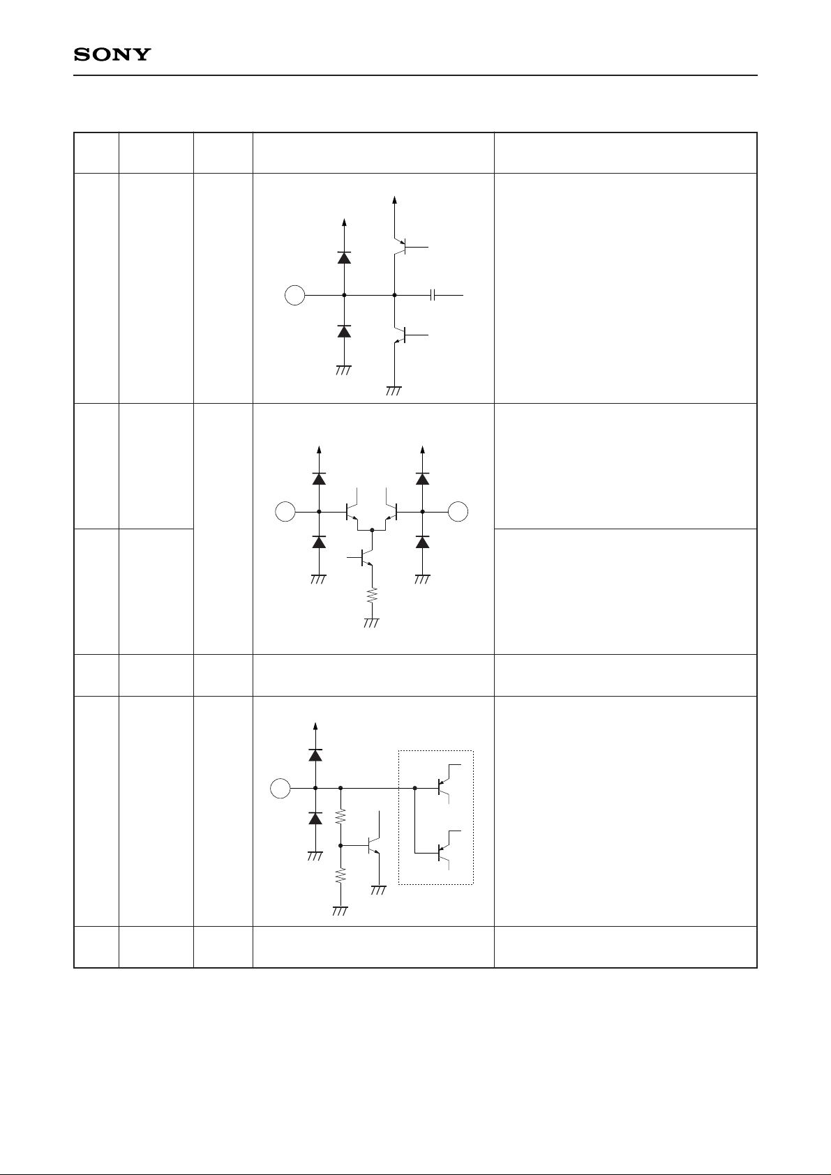
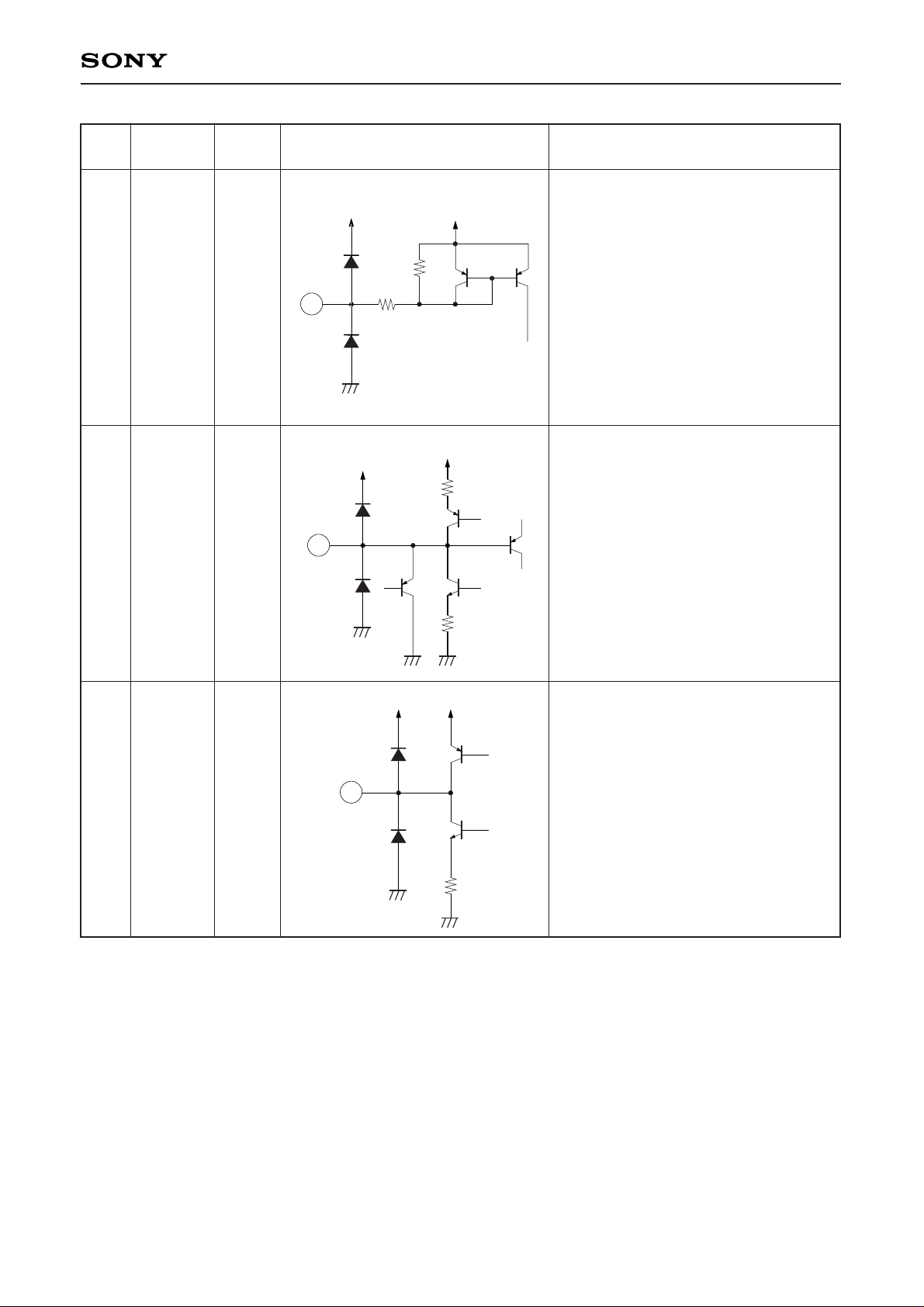
Equivalent circuit Description
Output pin of built-in operational
amplifier
Non-inverting input pin of operational
amplifier
Inverting input pin of operational
amplifier
Power supply input to DC-DC controller
circuits
Reference Voltage
Power supply input to pre-driver circuits
1
VCC1
VCC1
VCC1 VCC1
2
48
VCC2
4
30k
75k
× 4
—5—
CXA2534Q
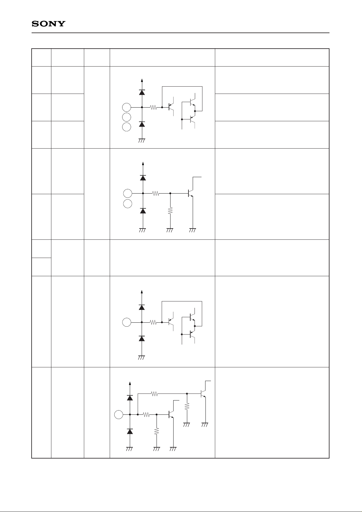
Pin
No.
6
7
9
8
10
11
28
12
13
Symbol
TRACK IN
FOCUS IN
SLED IN
FT MUTE
SL BRAKE
PGND
SP IN
SP MUTE
Pin
Voltage
1.6 V
0 V
0 V
1.6 V
0 V
Equivalent circuit Description
Tracking error signal input pin
Focus error signal input pin
Sled error signal input pin
Focus and Tracking mute input pin
Sled motor brake input pin
Power ground for H-bridge drivers
Spindle error signal input pin
Spindle mute input
VCC2
11k
6
7
9
VCC2
75k
75k
8
10
VCC2
7.5k
12
VCC2
75k
75k
75k
75k
13
—6—
CXA2534Q
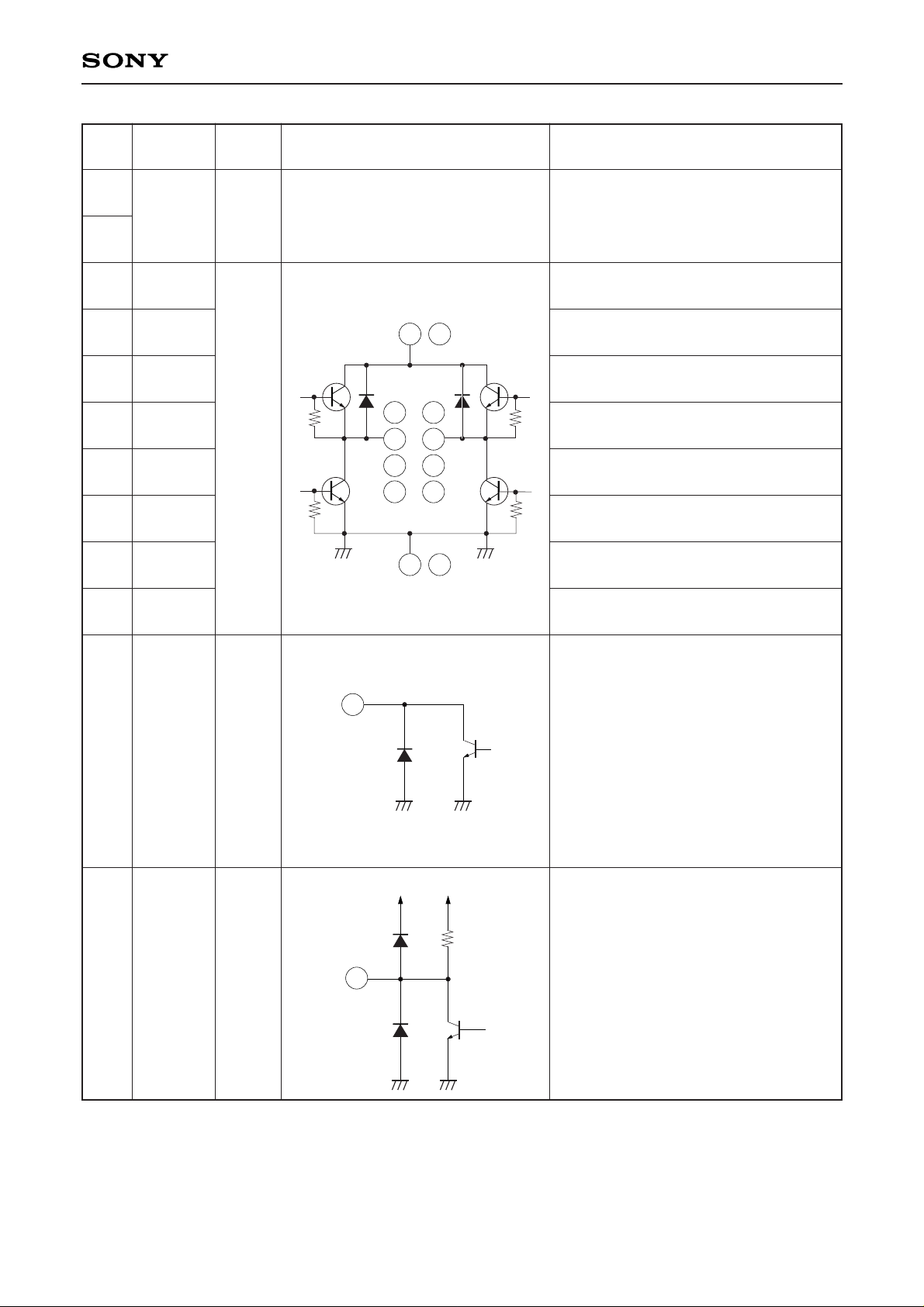
Pin
No.
14
19
15
16
17
18
20
21
22
23
24
25
Symbol
PVCC
TRACK–
TRACK+
FOCUS–
FOCUS+
SLED–
SLED+
SP–
SP+
EMP
RESET
Pin
Voltage
—
—
—
VCC1
Equivalent circuit Description
Power supply input for H-bridge drivers
Negative output pin to tracking motor
Positive output pin to tracking motor
Negative output pin to focus motor
Positive output pin to focus motor
Negative output pin to sled motor
Positive output pin to sled motor
Negative output pin to spindle motor
Positive output pin to spindle motor
Battery empty detection output pin
Reset output pin
24
16
18
20
22
15
17
19
21
11
14 19
28
VCC1 VCC1
90k
25
—7—
CXA2534Q
Pin
No.
26
27
29
Symbol
OFF
PWMFIL
PSW
Pin
Voltage
VCC1
—
—
Equivalent circuit Description
Input pin to put IC into standby mode
PWM filter pin
PWM switching output pin
VCC1
VCC1
30k
180k
26
VCC2
VCC2
2k
2k
27
BATT BATT
15
29
 Loading...