

Sony CXA2525AN, CXA2525AM Datasheet

– 1 –
CXA2525AM/AN
E96318C8Z
RF Amplifier for CD Player and CD-ROM
Description
The CXA2525AM/AN is an IC for RF signal
processing of CD player and CD-ROM.
Features
• Wide-band RF amplifier. (RF signal fc ≥ 12MHz)
• RF equalizer (T type)
• EFM time constant can be adjusted
(with switching function)
• APC (Automatic Power Control) function
• Power saving function
Functions
• RF summing amplifier
• RF equalizer
• Focus error amplifier
• Tracking error amplifier
• APC circuit
Absolute Maximum Ratings
• Supply voltage VCC 7V
•Storage temperature Tstg –65 to +150 °C
• Allowable power dissipation
PD 500 mW
Operating Conditions
• Supply voltage VCC – GND +3.0 to +5.5 V
• Operating temperature Topr –20 to +75 °C
Applications
• CD players
• CD-ROM drives
Sony reserves the right to change products and specifications without prior notice. This information does not convey any license by
any implication or otherwise under any patents or other right. Application circuits shown, if any, are typical examples illustrating the
operation of the devices. Sony cannot assume responsibility for any problems arising out of the use of these circuits.
CXA2525AM
20 pin SOP (Plastic)
CXA2525AN
20 pin SSOP (Plastic)
For the availability of this product, please contact the sales office.
– 2 –
CXA2525AM/AN
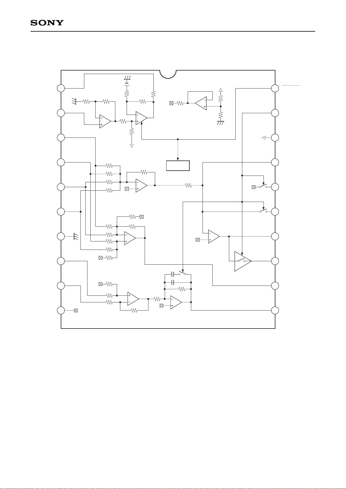
Block Diagram
LD
PD
A
B
C
D
GND
E
F
VC
APC_ON
MODE
VCC
RF_M
BPF_SW
LPF_SW
RFO_1
RFO_2
FE
TE
2
3
4
5
6
7
8
9
10
1
11
12
13
14
15
16
17
18
19
20
BGR
VC
BUFFER
40k
40k
V
CC
25
1k
10k
V
CC
56k
10k
55k 56k10k
1.25V
APC
Standby
10k
10k
10k
10k
10k
64k
64k
64k
64k
174k
348k
348k
2k
VC
V
CC
RF
Summing
Amp
Focus
Error Amp
RF Drive
Amp
VC
11p
5p
320k
VC
VC
112k
73.4k
112k
44k
44k
Tracking
Error Amp
Tracking
Drive Amp
– 3 –
CXA2525AM/AN
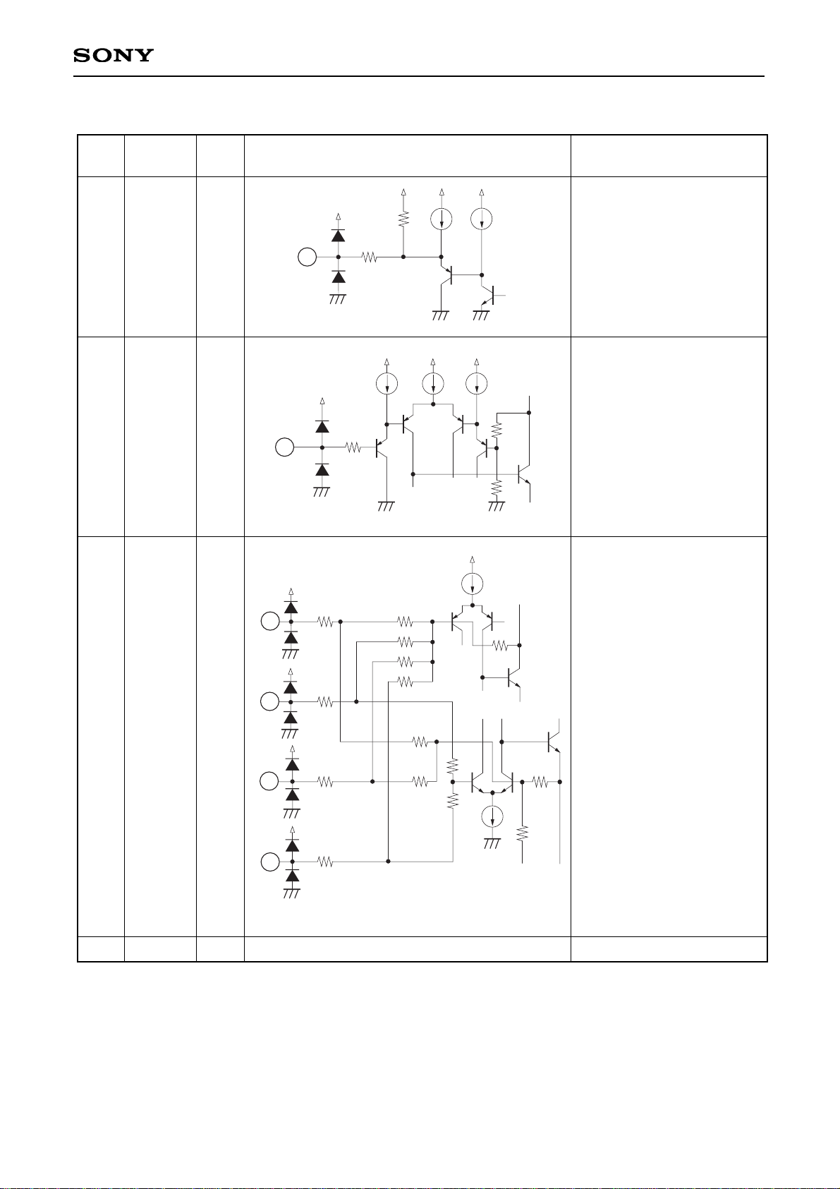
Pin Description
Pin
No.
Symbol I/O Equivalent circuit Description
1
LD
O
APC amplifier output.
1k
1
10k
2
PD
I
APC amplifier input.
7
GND
Ground.
8k
55k
10k
2
3
4
5
6
A
B
C
D
I
I
I
I
Input of RF summing
amplifier and focus error
amplifier.
10k
10k
10k
10k
10k
3
4
5
6
124
124
124
124
64k
64k
64k
64k
348k
348k
– 4 –
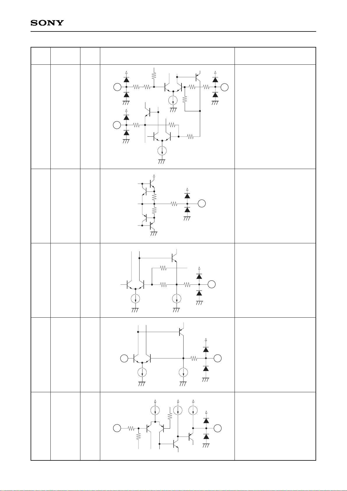
CXA2525AM/AN
8
9
11
E
F
TE
I
I
O
Tracking error amplifier input
for Pins 8 and 9;
tracking error drive output for
Pin 11.
8
9
11
124
44k
112k
124
44k
112k
320k
73.4k
124
10
VC
O
(VCC + GND) / 2 DC voltage
output.
120
120
25
10
12
FE
O
Focus error amplifier output
for Pin 12.
12
348k
348k
124
13
RFO_2
O
Buffer switch output which
sets the RF signal time
constant.
OFF when Pin 19 is
connected to VCC, ON when
it is connected to GND.
124
13
14
14
17
RFO_1
RF_M
O
I
Non-inversion input of RF
drive amplifier for Pin 17;
RF signal output for Pin 14;
resistance value connected
between Pins 14 and 17
which determines the low
frequency gain of RF drive
amplifier.
14
17
124
2k
1k
Pin
No.
Symbol I/O Equivalent circuit Description
 Loading...