

Sony CXA2513M Datasheet

3-Band Preset Graphic Equalizer IC (with standby and memory on last preset mode)
Description
The CXA2513M is a 3-band preset graphic equalizer
developed for stereo set, cassette tape recorder with
radio, etc. It has 5 modes: FLAT, ROCK, VOCAL,
POP and JAZZ. The selection is via 5 control pins.
The center frequencies of three bands are 100Hz,
1kHz and 10kHz. The center frequencies of these
bands are determined by 2 external resistors. It also
has a standby feature. When the standby pin goes
low, the IC stores the last preset mode. When this
pin goes high, the IC restores the last preset mode
before standby. It can be initialized to any one of the
two preset modes (FLAT, ROCK) upon power up.
Features
• Very few external parts
• 3-band monolithic filters (100Hz, 1kHz, 10kHz)
• The center frequencies of the band-pass filters can
be adjusted
• 5 preset modes (FLAT, ROCK, VOCAL, POP, JAZZ)
• Equips with output ports to drive external LEDs
• Mute pulse output pin
• Standby feature with last preset mode memory
• Can be initialized to one of the two preset modes
(FLAT or ROCK)
Applications
Preset graphic equalizer for cassette tape recorder
with radio and portable stereo
Structure
Bipolar silicon monolithic IC
Absolute Maximum Ratings (Ta = 25°C)
• Supply voltage VCC 12 V
• Allowable power dissipation PD 600 mW
• Storage temperature Tstg –65 to +150 °C
Recommended Operating Conditions
• Supply voltage VCC 4.5 to 10 V
• Operating temperature Topr –20 to +75 °C
– 1 –
E97741-PS
Sony reserves the right to change products and specifications without prior notice. This information does not convey any license by
any implication or otherwise under any patents or other right. Application circuits shown, if any, are typical examples illustrating the
operation of the devices. Sony cannot assume responsibility for any problems arising out of the use of these circuits.
CXA2513M
20 pin SOP (Plastic)

– 2 –
CXA2513M
Block Diagram and Pin Configuration
2
3
4
5
6
7
8
9
10
11
12
13
14
15
16
17
18
19
20
1
VOCAL
FLAT
JAZZ
POP
MUTE DET+
ROCK
MUTE DET–
FLAT INIT
STANDBY
TIMING CAP
V
CC
GND
IN2
IN1
LOW-FREQ
ISET
MUTE
REF
OUT2
OUT1
MUTE
DETECTOR
GRAPHIC
EQUALIZER
14dB
CURRENT
CONTROL
GRAPHIC
EQUALIZER
BIAS
14dB
INITIAZATION
MODE
LATCH
&
MEMORY
INITIALIZATION
MODE AND
STANDBY
– 3 –
CXA2513M
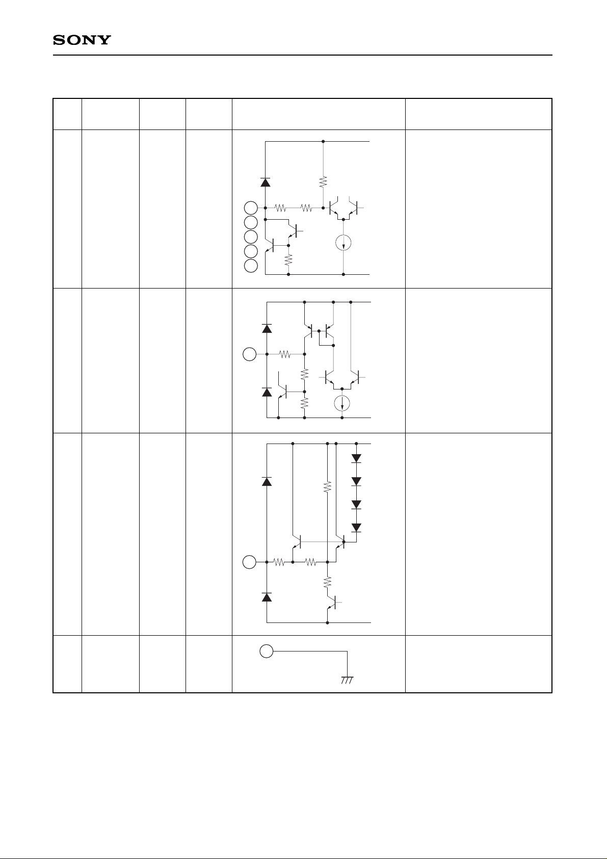
Pin Description
Pin
No.
1
2
3
19
20
FLAT
POP
ROCK
JAZZ
VOCAL
Mode selection input pins with
LED driving capability.
Flat initialization pin.
If the pin is connected to a
220nF capacitors, it initializes
to FLAT mode.
If the pin is not connected, it
initializes to ROCK mode.
Timing capacitor pin.
It is connected to a capacitor.
The charging and discharging
of this capacitor will determine
the timing of the logic control.
GND pin.
VCC or
1V
—
—
—
—
VCC –
5∗VBE
GND
FLAT
INIT
TIMING
CAP
GND
4
5
6
Symbol Voltage
I/O
resistance
Equivalent circuit Description
2
3
19
20
1
147 50k
50k
20k
GND
V
CC
GND
V
CC
147
20k
20k
4
5
GND
V
CC
147 150k
20k
100k
6
GND
– 4 –
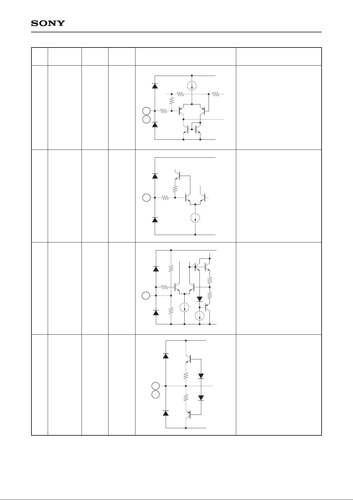
CXA2513M
Pin
No.
714IN1
IN2
Signal input pin.
VCC/2
50k
Symbol Voltage
I/O
resistance
Equivalent circuit Description
7
14
GND
V
CC
50k
147
5k 11.5k
8 ISET
Reference current setting pin
(for graphic equalizer).
Normally 160kΩ resistor is
connected.
1.2V —
GND
V
CC
147
300
8
9 REF
Signal reference voltage pin.
A capacitor is connected for
ripple rejection.
VCC/2 40k
GND
V
CC
9
147
80k
80k
300
300
1011OUT1
OUT2
Signal output pin.
VCC/2 0
11
GND
V
CC
10
300
300
NPN
– 5 –
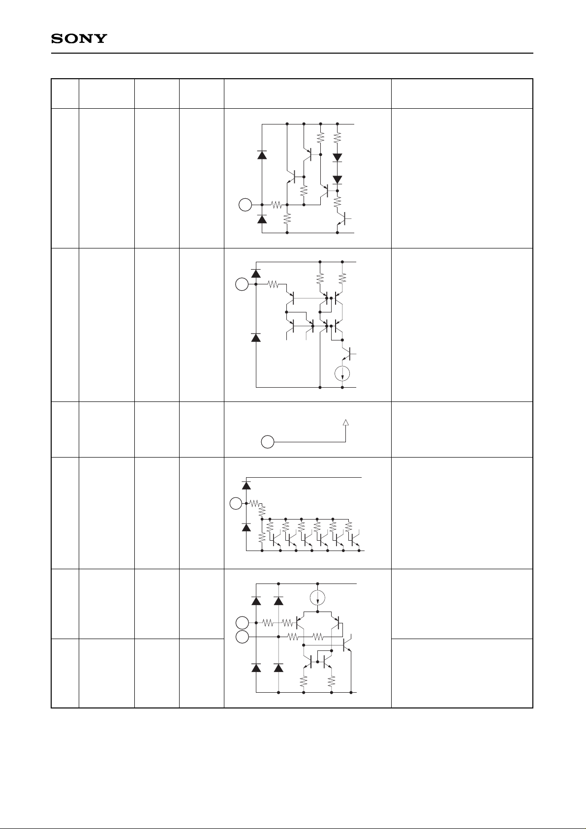
CXA2513M
Pin
No.
17
MUTE
DET–
Negative input of the mute
detector comparator.
Positive input of the mute
detector comparator.
—
—
18
MUTE
DET+
—
—
Symbol Voltage
I/O
resistance
Equivalent circuit Description
GND
V
CC
17
4k4k
10k
147
10k147
18
13
LOW
FREQ
Low frequency adjustment pin.
Set the center frequency of
the bass.
VCC 0
GND
V
CC
147
10k 7.5k
13
12
MUTE
Mute pulse output pin.
0 300k
GND
V
CC
15k
40k
40k
300k
12
40k
147
15 VCC Power supply pin.VCC —
15
V
CC
16
STAND
BY
Standby pin.
When not connected, the IC in
standby.
When connected to VCC, the
IC in normal operation
— 20k
GND
V
CC
16
147
20k
50k
5k 5k 5k 5k 5k 5k
– 6 –
CXA2513M
Electrical Characteristics (Ta = 27°C, VCC = 8V, C = 22µF)
Symbol
ICC (STANDBY)
ICC (FLAT)
Vout (max.)
GE (FLAT) B
GE (FLAT) M
GE (FLAT) T
GE (POP) M
GE (POP) T
GE (ROCK) B
GE (ROCK) T
GE (VOCAL) B
GE (VOCAL) M
GE (JAZZ) B
GE (JAZZ) M
GE (JAZZ) T
Bal
∆fO
THD
VNOIS (FLAT)
CS
PSRR
ILED
Vmute (off)
Vmute (on)
Vstandby (off)
Current consumption
Current consumption
Maximum output level
Balance
Center frequency deviation
Total harmonic distortion
Noise level
Channel separation
Power supply ripple
rejection
Maximum LED drive
current
Mute off voltage
Mute on voltage
Standby off voltage
Standby pin is low - No input
FLAT mode - No input
FLAT preset mode, f = 1kHz @
THD = 1%, RL = 10kΩ
Vin = 0.05Vrms, fO = 100Hz
Vin = 0.05Vrms, fO = 1kHz
Vin = 0.05Vrms, fO = 10kHz
Vin = 0.05Vrms, fO = 0.8 to 1.2kHz
Vin = 0.05Vrms, fO = 0.8 to 12kHz
Vin = 0.05Vrms, fO = 0.8 to 120Hz
Vin = 0.05Vrms, fO = 0.8 to 12kHz
Vin = 0.05Vrms, fO = 0.8 to 120Hz
Vin = 0.05Vrms, fO = 0.8 to 1.2kHz
Vin = 0.05Vrms, fO = 0.8 to 120Hz
Vin = 0.05Vrms, fO = 0.8 to 1.2kHz
Vin = 0.05Vrms, fO = 0.8 to 12kHz
GE (Out1) – GE (Out2)
RL = 10kΩ, FLAT preset mode,
f = 1kHz, Vin = 0.1Vrms
RL = 10kΩ, FLAT preset mode,
DIN AUDIO filter, Vin = 0Vrms
Vin = 0.1Vrms at 1kHz,
FLAT preset mode
Vin = 0.1Vrms at 100Hz,
FLAT preset mode
Current flowing through LED
connected to a switch depressed
Vm_det+ = 1/4VCC and
Vm_det– = 1/2VCC
Vm_det+ = 3/4VCC and
Vm_det– = 1/2VCC
ICC goes from standing to normal
operation
—
—
2.7
12.6
12.55
12.5
16.5
18.0
21.0
20.0
14.5
20.0
16.2
15.5
5.5
–1
–20
—
—
40
40
15
—
6.8
3
17.5
9.6
3.0
14.6
14.55
14.5
19.0
21.0
24.0
23.0
17.0
23.0
18.7
18.0
8.0
0
0
0.25
19
47
46
—
0
7.1
—
45.0
14.0
—
16.6
16.55
16.5
21.5
24.0
27.0
26.0
19.5
26.0
21.2
20.5
10.5
1
20
1
55
—
—
—
0.1
—
—
µA
mA
Vpeak
dB
dB
dB
dB
dB
dB
dB
dB
dB
dB
dB
dB
dB
%
%
µVrms
dB
dB
mA
V
V
V
Parameter Measurement conditions Min. Typ. Max. Unit
PRESETS
Normal
Bass
Mid
Treble
Mid Boost
Treble Boost
Bass Boost
Treble Boost
Bass Boost
Mid Boost
Bass Boost
Mid Boost
Treble Cut
POP
ROCK
VOCAL
JAZZ
 Loading...