Sony CXA2149Q Datasheet

—1—
E99946A9Y-TE
Sony reserves the right to change products and specifications without prior notice. This information does not convey any license by
any implication or otherwise under any patents or other right. Application circuits shown, if any, are typical examples illustrating the
operation of the devices. Sony cannot assume responsibility for any problems arising out of the use of these circuits.
Absolute Maximum Ratings
(Ta=25 °C unless stated)
• Supply voltage VCC 12 V
• Storage temperature Tstg –65 to +150 °C
• Allowable power dissipation
PD 900 mW
Operating Conditions
• Supply voltage VCC 9+/–0.5 V
• Typical supply current 75 mA
• Operating temperature Topr –20 to +75 °C
Description
The CXA2149Q is a video and audio switch IC
featuring I2C bus compatibility for TV’s. The IC has
input pins that are compatible with the SCART
protocols. It offers other features such as an
electronic mute function with switching noise
reduction (zero cross detection), electronic volume
control, automatic SYNC pulse detection, and group
delay control.
Features
• 3 CVBS inputs.
• 2 CVBS outputs.
• Group delay control on TV and CVIN1.
• SYNC ID on TV and CVIN1.
• 3 Y/C inputs.
• 2 Y/C outputs.
• 6 L/R/2 inputs.
• 3 L/R/2 outputs.
• Mode inputs compatible with the SCART protocol.
• 3 Y/C mixer circuits.
• Audio muting via software control.
• External muting input.
• Audio switching noise elimination circuit.
• Volume adjustment via software control on L/R
channel 3.
• Wide band video amplifiers (20 MHz, –3 dB).
• Wide audio dynamic range (3 Vrms typ)
• Serial control via I2C bus.
• Separate control of video and audio switches.
• High impedance maintained by I2C lines (SDA,
SCL) even when power is off.
• Configurable dual slave address 90/92.
• I2C bus 5 and 3.3 V compatible.
Applications
TV’s
Structure
Bipolar silicon monolithic IC
I2C-Bus-Compatible Audio/Video Switch
64 pin QFP (Plastic)
CXA2149Q
For the availability of this product, please contact the sales office.
—2—
CXA2149Q
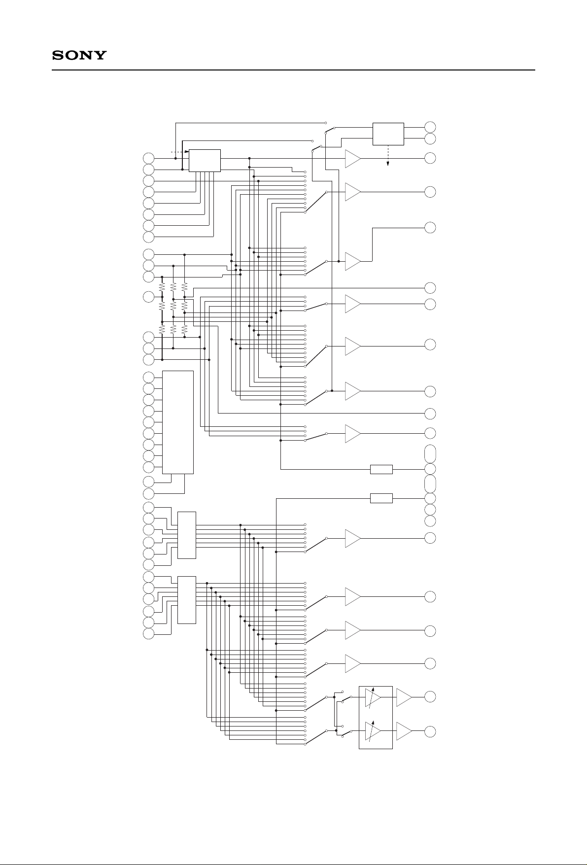
Block Diagram
REXT
TVOUT
RGD4
RGD3
LO0
RGD2
RGD1
LO1
CVOUT1
TRAP1
YOUT1
COUT1
SCL
SDA
ADR
MUTE
MODE1
MODE2
C2
C3
COUT2
TRAP2
YOUT2
DVCC
CVOUT2
DGND
LOUT2
ROUT2
LOUT1
ROUT1
RV1
RV2
RV3
RV4
RV5
RTV
AGND
LV1
LV2
LV3
LV4
LV5
LTV
ROUT3
LOUT3
ABIAS
AVCC
MODE3
C1
Y3
TRAP3
VBIAS
Y2
VGND1, 2
Y1
VVCC1, 2
CVIN2
TC2
CVIN1
TC1
TV
SYNC
DETECT
GROUP
DELAYS
I C
6dB
6dB
0dB
0dB
6dB
0dB
0dB
6dB
6dB
6dB
6dB
6dB
6dB
I C
LOGIC
BIAS
BIAS
–6dB
–6dB
0 to –63dB
0 to –63dB
38
39
40
41
21
23
24
2
9
11
10
13
45
47
46
43
59
12
55
57
22
31
61
63
1
3
4
6
7
60
62
64
54
53
56
58
49
51
52
14
15
16
17
18
19
42
44
20
5
8
25
26
27
28
29
30
33
34
35
36
37
32
2
I C
2
2
,
48
,

—3—
CXA2149Q
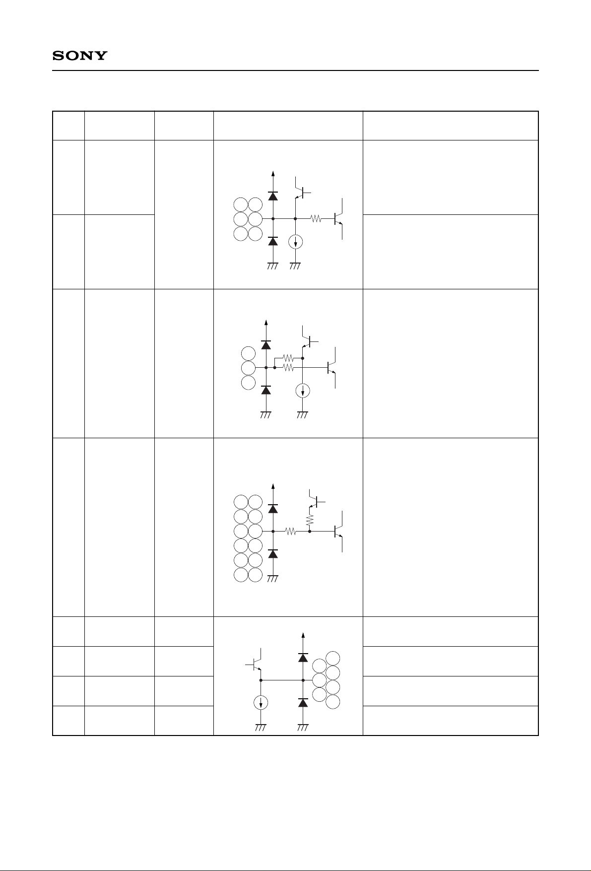
Pin Configuration
1 2 3 4 5 6 7 8 9
10 11 12
13
14 15 16 17 18 19
33343536373839404142434445464748495051
REXT
TVOUT
RGD4
RGD3
LO0
RGD2
RGD1
LO1
CVOUT1
TRAP1
YOUT1
VVCC2
COUT1
SCL
SDA
ADR
MUTE
MODE1
MODE2
C2
NC
C3
VGND2
COUT2
TRAP2
YOUT2
DVCC
CVOUT2
DGND
LOUT2
ROUT2
LOUT1
ROUT1
RV1
RV2
RV3
RV4
RV5
52
53
54
55
56
57
58
59
60
61
62
63
64 20
21
22
23
24
25
26
27
28
29
30
31
32
RTV
AGND
LV1
LV2
LV3
LV4
LV5
LTV
ROUT3
LOUT3
ABIAS
AVCC
MODE3
C1
TRAP3
Y3
VBIAS
Y2
VGND1
Y1
VVCC1
CVIN2
TC2
CVIN1
TC1
TV
CXA2149Q
—4—
CXA2149Q
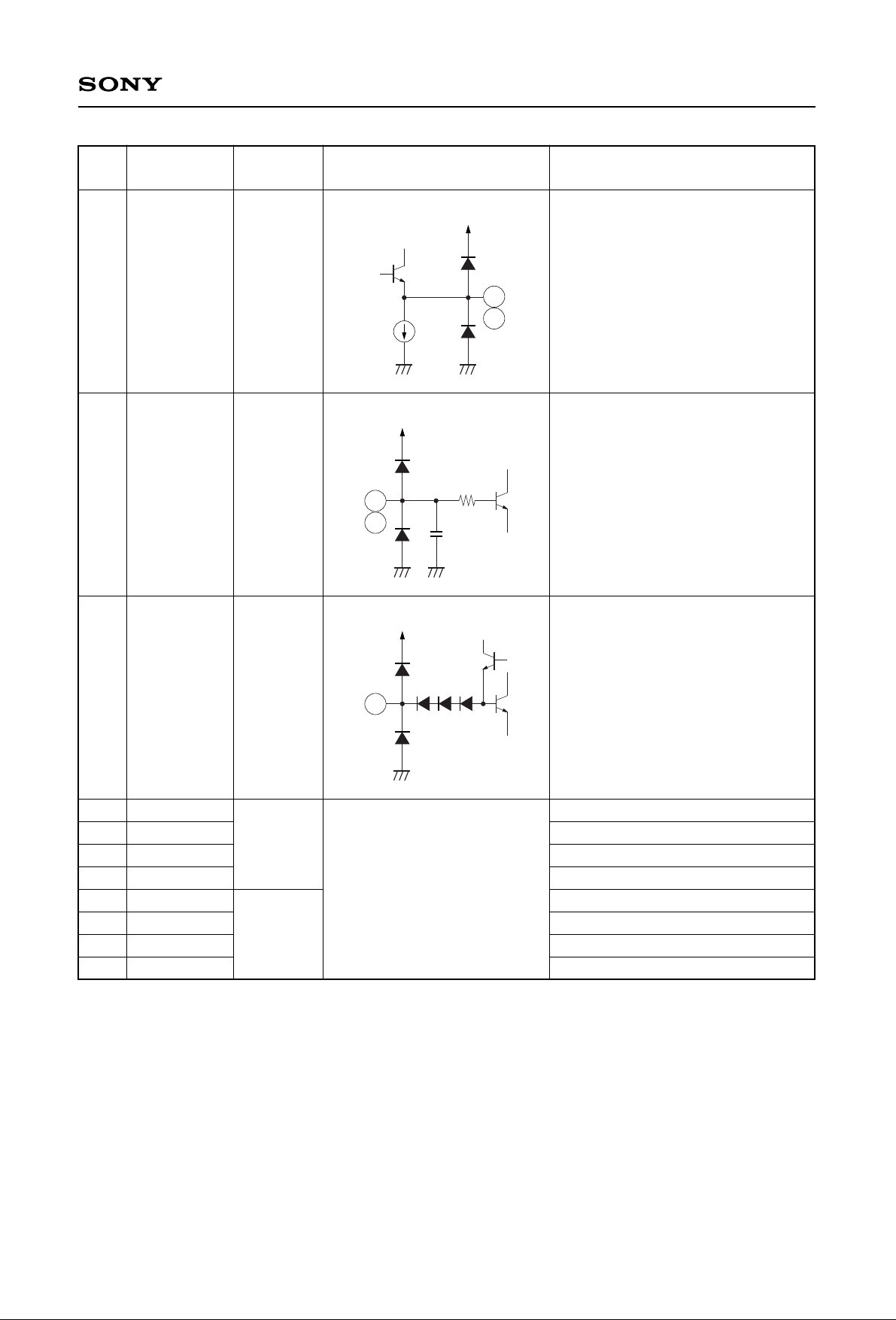
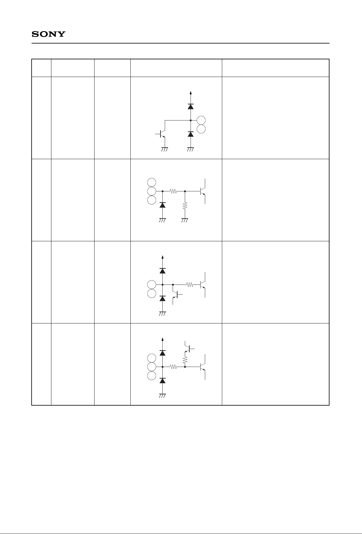
Pin Description
64
62
60
58
56
54
52
51
49
25
30
29
28
27
26
32
37
36
35
34
33
9
43
11
45
13
47
2
TV
CVIN1
CVIN2
Y1
Y2
Y3
C1
C2
C3
LTV
LV1
LV2
LV3
LV4
LV5
RTV
RV1
RV2
RV3
RV4
RV5
CVOUT1
CVOUT2
YOUT1
YOUT2
COUT1
COUT2
TVOUT
3.9
4.5
4.5
3.8
3.5
4.5
3.8
Pin
Symbol
Pin
Equivalent circuit Description
No voltage (V)
54
56
58
60
62
64
VCC
0.5µ
147
VCC
100µ
147
20k
49
51
52
5.2V
VCC
33k
33k
4.5V
25
26
27
28
29
30
32
33
34
35
36
37
VCC
1.8m
2
9
11
13
43
45
47
Video signal inputs.
Luminance signal inputs.
Chrominance signal inputs.
Audio signal inputs.
Composite video signal outputs.
Luminance signal outputs.
Chrominance signal outputs.
TV signal group delayed output.
—5—
CXA2149Q
7
3
6
4
1
44
59
12
21
42
57
48
31
RGD1
RGD4
RGD2
RGD3
REXT
DVCC
VVCC1
VVCC2
AVCC
DGND
VGND1
VGND2
AGND
4.5
4.5
1.7
9
0
Pin
Symbol
Pin
Equivalent circuit Description
No voltage (V)
VCC
0.5m
3
7
VCC
1.7k
4
6
VCC
3.8V
1
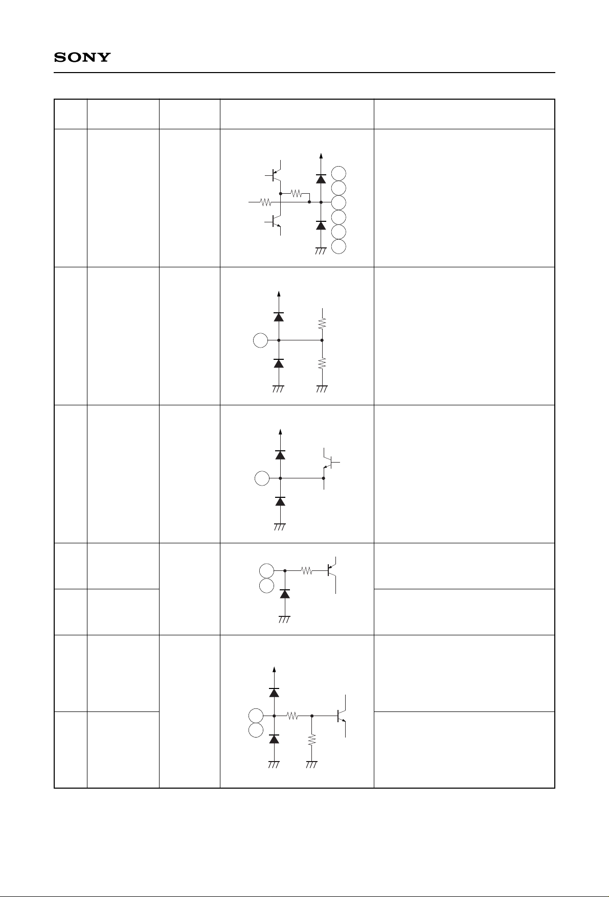
Group delay output to external
filter.
Group delay inputs from external
filter.
Pin connection for 39 kΩ group delay
setting resistor. Pin voltage is group
delay control dependent.
Digital supply.
Video supply.
Video supply.
Audio supply.
Digital ground.
Video ground.
Video ground.
Audio ground.
—6—
CXA2149Q
39
41
23
38
40
24
22
55
14
15
16
17
LOUT1
LOUT2
LOUT3
ROUT1
ROUT2
ROUT3
ABIAS
VBIAS
SCL
SDA
ADR
MUTE
4.5
4.5
4.5
Pin
Symbol
Pin
Equivalent circuit Description
No voltage (V)
VCC
4.5V
22
20k
20k
VCC
4.5V
55
14
15
4k
Audio signal outputs.
Internal reference bias for audio
circuits. A capacitor is connected
from this pin to GND.
Internal reference bias for video
circuits. A capacitor is connected
from this pin to GND.
I2C bus clock line.
I2C bus data line.
Slave address control.
Audio signal output mute.
VCC
72k
28k
16
17
VCC
23
24
38
39
40
41
56
20k
—7—
CXA2149Q
5
8
18
19
20
63
61
10
46
53
LO0
LO1
MODE1
MODE2
MODE3
TC1
TC2
TRAP1
TRAP2
TRAP3
5
3.5
Pin
Symbol
Pin
Equivalent circuit Description
No voltage (V)
VCC
5
8
I C
control
2
25k
25k
19
18
20
VCC
147
61
63
VCC
200
200
46
10
53
Open collector logic outputs.
Function SCART inputs from SCART
connectors.
Video detect time constant capacitor
connection pins.
Connects trap circuit for subcarrier.
Note. Pin voltages indicated the approximate DC voltage levels with no signals inputs.

—8—
CXA2149Q
Electrical Characteristics (Ta=25 °C, VCC=9 V unless stated.)
Item
Supply voltage
Supply current
Symbol
VCC
ICC
Conditions Min. Typ. Max. Unit
8.5 9.0 9.5 V
40 75 100 mA
I2C (Operation of the I2C using either a 3.3 or 5 V supply on the external controller is possible)
Item
High level input voltage
Low level input voltage
Low level output voltage
Max. clock frequency
Min. waiting time for data change
Min. waiting time for data transfer start
Low level clock pulse width
High level clock pulse width
Min. waiting time for start preparation
Min. data hold time
Min data preparation time
Rise time
Fall time
Min. waiting time for stop preparation
Symbol
VIH
VIL
VOL
fSCL
tBUF
tHDSTA
tL
tH
tSUSTA
tHDDAT
tSUDAT
tR
tF
tSUSTO
Conditions
SDA 3 mA sink
Min. Typ. Max. Unit
2.3 — 5 V
0 — 1.5 V
0 — 0.4 V
0 — 100 kHz
4.5 — — µs
4 — — µs
4.7 — — µs
4 — — µs
4.7 — — µs
5 — — s
250 — — ns
— — 1 µs
— — 300 ns
4.7 50 — µs
 Loading...