

Sony CXA2126Q Datasheet

Audio/Video Switch with Electronic Volume for 2 Scart
Description
The CXA2126Q is an I2C programmable audio, video
switch designed primarily for set top box applications. It
interfaces from digital encoder sources to TV and VCR
scart connectors.
Features
• 2 scart independent audio/video switching (TV, VCR)
• Compatible with 3 scart Audio/Video switch,
CXA2125Q
• 0 to –63dB volume control with click noise reduction
• 3 stereo audio inputs
• I2C control
• Scart Function Switching input and output
• Scart Fast Blanking for OSD
• Mono switchable to stereo on TV and VCR outputs
• On-chip +12V to +9V voltage regulator
• Logic output
• Selectable +6dB, +12dB gain on TV output
• RGB input on VCR scart
Applications
Digital Set Top Box
Structure
Bipolar silicon monolithic IC
Absolute Maximum Ratings
• Supply voltage VCC 12 V
• Operating temperature Topr –20 to +75 °C
• Storage temperature Tstg –65 to +150 °C
• Allowable power dissipation
PD 850 mW
Operating Conditions
• Supply voltage 10.7 to 12 V
• Operating voltage 9 ± 0.5 V
– 1 –
E99339-PS
Sony reserves the right to change products and specifications without prior notice. This information does not convey any license by
any implication or otherwise under any patents or other right. Application circuits shown, if any, are typical examples illustrating the
operation of the devices. Sony cannot assume responsibility for any problems arising out of the use of these circuits.
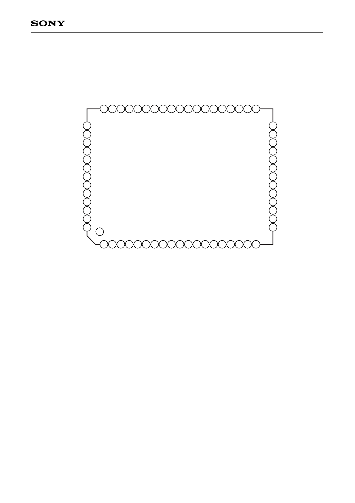
CXA2126Q
64 pin QFP (Plastic)
– 2 –
CXA2126Q
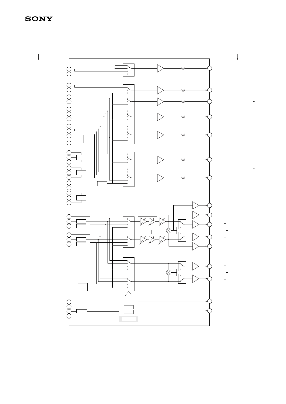
Block Diagram
× 2
× 2
ROUT1
34
LOUT1
36
8dB 1dB 0/6dB
MONO SWITCH
Selectable Gain Stage
MONO SWITCH
× 2
× 2
× 2
× 2
× 2
FBLK_IN1DIG
Typical Connection
VCR
DIG BLUE
VCR BLUE
DIG GREEN/CVBS
VCR GREEN
DIG RED/CHROMA
DIG CHROMA
VCR RED/CHROMA
DIG CVBS/LUMA
DIG CVBS/LUMA
VCR CVBS/LUMA
TV CVBS
TV_FBLANK
+5V
0V
FBLK_IN2
FBLK_SW
100Ω
VIN1
VIN2
VIDEO_SWITCH1 (TV)
VIN3
VIN4
VIN5
VIN6
VIN7
VIN8
VIN9
VIN10
VIN11
VIDEO_SWITCH2 (VCR)
AUDIO_SWITCH1 (TV)
VOLUME CONTROL
& MUTE
8dB
ZCD
1dB 0/6dB
52
53
63
61
2
59
4
6
57
8
10
55
23
VID_V
CC
VID_BIAS
VID_GND
60
62
7
Bias
Mute
Bias
4.5V
Mute
Bias 1
4.05V
AUD_VCC
DIG_VCC
AUD_BIAS
AUD_GND
DIG_GND
20
19
26
Bias 2
4.5V
VCC_12V
VREG_BASE
VREG_9V
58
56
38
43
54
RIN1 (DIG)
3
RIN2 (VCR)
12
RIN3 (TV)
22
9V reg
–6dB
–6dB
LIN1 (DIG)
5
LIN2 (VCR)
14
LIN3 (TV)
24
–6dB
–6dB
SDA
11
SCL
9
FNC_VCR
64
HW_MUTE
45
Monitor
TV BLUE
TV GREEN
TV RED/C
TV CVBS/Y
VCR CHROMA
VCR CVBS/Y
Typical Connection
50
VOUT1
100Ω
48
× 2
VOUT2
100Ω
47
× 2
VOUT3
100Ω
46
× 2
VOUT4
100Ω
49
× 2
VOUT5
100Ω
41
× 2
VOUT6
100Ω
44
FNC_TV
30
LOGIC
28
× 2
MONO
33
PHONO_R
35
RTV
40
LTV
TV
42
PHONO_L
37
AUDIO_SWITCH2 (VCR)
I2C
Interface
LOGIC
P.O.D
VCR
TV
VCR
3.3V or 5V
– 3 –
CXA2126Q
1 2 3 4 5 6 7 8 9 10 11 12 13 14 15 16
20
21
22
23
24
25
26
27
28
29
30
31
32
36373839404142434445464748495051
52
53
54
55
56
57
58
59
60
61
62
63
64
FBLK_IN1
FBLK_IN2
VREG_9V
VIN10
VREG_BASE
VIN7
V
CC_12V
VIN4
VID_V
CC
VIN2
VID_BIAS
VIN1
FNC_VCR
NC
VIN3
RIN1
VIN5
LIN1
VIN6
VID_GND
VIN8
SCL
VIN9
SDA
RIN2
NC
LIN2
NC
NC
17 18 19
NC
NC
AUD_BIAS
NC
TV_FBLANK
VOUT4
VOUT1
VOUT2
VOUT3
HW_MUTE
VOUT6
DIG_GND
LTV
VOUT5
RTV
NC
DIG_V
CC
PHONO_L
LOUT1
333435
PHONO_R
ROUT1
MONO
NC
NC
FNC_TV
NC
LOGIC
NC
AUD_GND
NC
LIN3
VIN11
RIN3
NC
AUD_V
CC
∗
NC = No connect
Pin Configuration
– 4 –
CXA2126Q
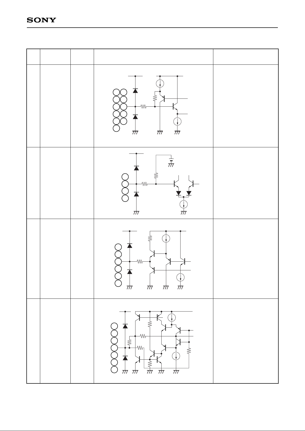
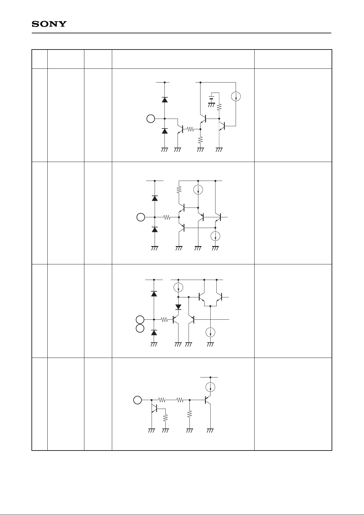
Pin Description
Pin
No.
Symbol
Pin
voltage
Equivalent circuit Description
63
61
2
59
55
23
4
6
57
8
10
V
CC = 12V VCC = 9V
14µA
120kΩ
147Ω
60µA
VIN1
VIN2
VIN3
VIN4
VIN5
VIN6
VIN7
VIN8
VIN9
VIN10
VIN11
4.6V
Video signal inputs.
An input coupling
capacitor is required.
(typ = 0.47µF)
63
61
2
59
4
6
57
8
10
55
23
12
22
14
24
V
CC = 12V
33kΩ
33kΩ
7µA
4.5V
RIN2
RIN3
LIN2
LIN3
4.5V
Audio signal inputs.
An input coupling
capacitor is required.
(typ = 2.2µF)
12
22
14
24
48
47
46
49
41
44
V
CC = 12V VCC = 9V
140µA
280µA
200Ω
100Ω
VOUT1
VOUT2
VOUT3
VOUT4
VOUT5
VOUT6
3.9V
Video signal outputs.
48
47
46
49
41
44
35
37
33
40
34
42
36
VCC = 12V VCC = 9V
55Ω
20kΩ
22kΩ
20kΩ
33µA
33µA
RTV
ROUT1
LTV
LOUT1
PHONO_R
PHONO_L
MONO
4.5V
Audio signal outputs.
A coupling capacitor may
be used.
(typ = 10µF)
40
34
42
36
35
37
33
– 5 –
CXA2126Q
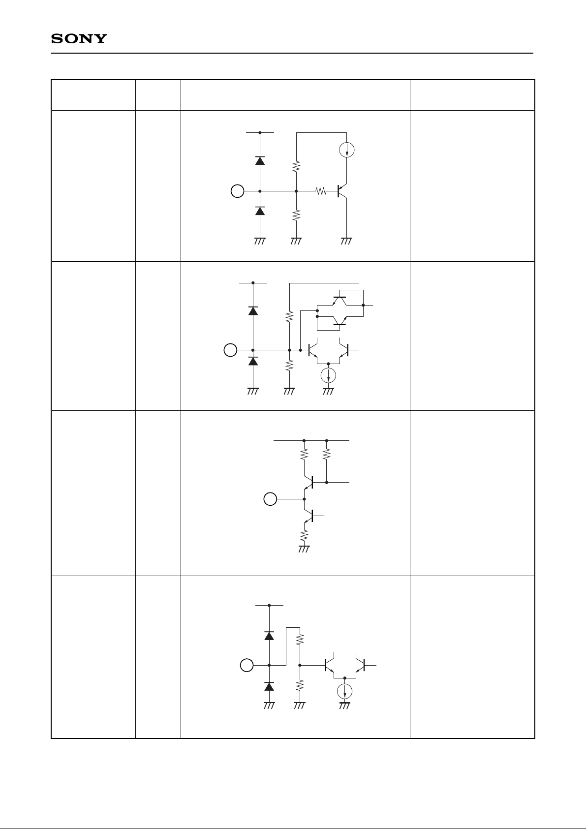
Pin
No.
Symbol
Pin
voltage
Equivalent circuit Description
62
V
CC = 12V VCC = 9V
14µA
11kΩ
9kΩ
200Ω
BIAS_
VIDEO
3.9V
Reference Bias for video
circuit.
Connected to GND with
capacitor.
(typ = 47µF)
62
7µA
19
V
CC = 12V VCC = 9V
20kΩ
20kΩ
BIAS_
AUDIO
4.5V
Reference Bias for audio
circuit.
Connected to GND with
capacitor.
(typ = 22µF)
19
30
V
CC = 12V
120Ω
3kΩ
15kΩ
FNC_TV
—
I2C controlled output
giving 0V, 6V or 12V.
30
120µA
54
V
CC = 12V
77.7kΩ
13.5kΩ
VREG_9V
9V
Pin connected to emitter
of external regulator
transistor.
54

– 6 –
CXA2126Q
Pin
No.
Symbol
Pin
voltage
Equivalent circuit Description
56
V
CC = 12V VCC = 12V
1mA
120µA
413Ω
15pF
VREG_
BASE
9.7V
Connection to base of
external regulator
transistor.
Max I = 1mA
56
9
VCC = 9V
40µA
4kΩ
10kΩ
40kΩ
SCL
—
I2C clock input.
9
11
VCC = 9V
40µA
4kΩ
4.5kΩ
40kΩ
SDA
—
I2C data input/output.
11
VCC = 12V
45
147Ω
28kΩ
72kΩ
HW_MUTE
—
HW MUTE: This pin is
active high > 2.5V < 9V.
When high, all audio
outputs are muted.
45
– 7 –
CXA2126Q
Pin
No.
Symbol
Pin
voltage
Equivalent circuit Description
28
V
CC = 12V VCC = 9V
8µA
7.5kΩ
3V
4.5kΩ
40kΩ
LOGIC
—
Open collector logic pins.
28
50
V
CC = 12V VCC = 9V
100µA
100µA
100Ω
100Ω
FBLK_
OUT
—
Fast Blank output set by
I2C to input FBLK_IN1 or
FBLK_IN2.
High = 5.3V
Low = 1.2V
Connected to external
emitter follower.
50
52
53
VCC = 12V
VCC = 9V
147Ω
90µA
50µA
FBLK_IN1
FBLK_IN2
—
Fast Blank inputs.
Low = < 0.4V
High = > 1.0V, < 3.0V
52
53
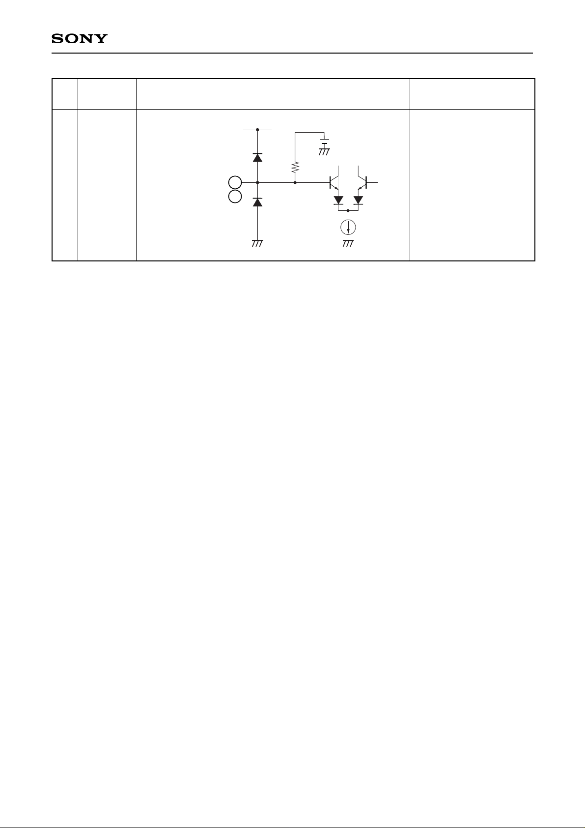
80µA
64
12.5kΩ 12.5kΩ
10kΩ
25kΩ
VCC = 9V
FNC_VCR —
Function switching input.
(Scart pin 8)
64
– 8 –
CXA2126Q
Pin
No.
Symbol
Pin
voltage
Equivalent circuit Description
3
5
V
CC = 12V
33kΩ
7µA
4.5V
RIN1
LIN1
4.5V
Audio signal inputs.
A coupling capacitor is
required for these inputs.
(typ = 2.2µF)
3
5

– 9 –
CXA2126Q
Electrical Characteristics
Nominal conditions (Ta = 25°C)
VCC_12V = 12V, No signal, no load
Current consumption ICC 30 50 80 mA
Item Symbol Conditions Min. Typ. Max. Unit
Video system Nominal conditions (Ta = 25°C, Vcc_12V = 12V, VREG_9V = 9V)
Input pin voltage
Output pin voltage – with
output on.
Output pin voltage – with
output off.
Gain
Bandwidth
Input dynamic range
Output dynamic range
Cross talk
S/N ratio
Input impedance
Non-linearity
Differential gain
Differential phase
Sync crush
VVPin
VVPout1
VVPout2
GVv
fV3dB
VDRVI
VDRVO
Vctv
S/NV
ZinV
Lin
DG
DP
SC
4.3
3.6
—
5.5
15
2.5
5.0
—
—
80
–3
–3
–3
–2
4.6
3.9
0
6.0
20
—
—
—
72
120
–0.4
1.5
1
0
4.9
4.2
0.5
6.5
—
—
—
–50
—
175
3
2
2
2
V
V
V
dB
MHz
Vp-p
Vp-p
dB
dB
kΩ
%
%
Deg
%
Item Symbol Conditions Min. Typ. Max. Unit
V2
V1 × 2
No signal, no load (Fig.1)
No signal, no load (Fig.1)
No signal, no load (Fig.1)
f = 200kHz, 0.3Vp-p input (Fig.2)
0.3Vp-p input, frequency where output
level is –3dB with 200kHz serving as
0dB (Fig. 2)
200kHz input (Fig.2)
200kHz, 2.5Vp-p input (Fig.2)
f = 4.43MHz, 1Vp-p input (Fig.2)
Ratio of 0.7Vp-p white video signal to
"black line" noise. Weighted using CCIR
567. HPF @5kHz, LPF @5MHz. (Fig.2)
1Vrms 1kHz input through 56kΩ.
Attenuation measured to calculate ZinV
(Fig.3)
(Fig.4)
V1 = Pin voltage +0.5V,
V2 = Pin voltage +1V
At output, non-linearity = –1 × 100
1.7Vp-p 5-step modulated staircase.
(Chroma and Burst are 150mVp-p
4.43MHz) (Fig.2)
as above. (Fig.2)
Percentage reduction in sync pulse
(0.4Vp-p), with tip at –1.2V input offset.
(Fig.4)
V2
V1
Input Pin V
Plus
– 10 –
CXA2126Q
Audio system
Unless otherwise stated: input coupling capacitor 1µF; output coupling capacitor of 10µF; load of 10kΩ.
Nominal conditions (Ta = 25°C, Vcc_12V = 12V, VREG_9V = 9V)
No signal, no load (Fig. 5)
f = 1kHz, 0.5Vrms input.
TV output amplifier set to 0dB (Fig. 6)
f = 1kHz, 0.5Vrms input.
TV output amplifier set to +6dB (Fig. 6)
f = 1kHz, 1Vrms input. (Fig. 6)
f = 1kHz, 0.5Vrms stereo input.
TV output amplifier set to 0dB (Fig. 6)
f = 1kHz, 0.5Vrms stereo input.
TV output amplifier set to +6dB (Fig. 6)
f = 1kHz, 0.5Vrms stereo input. (Fig. 6)
f = 1kHz, 1Vrms input.
TV output amplifier set to 0dB (Fig. 6)
f = 1kHz, 1Vrms input.
TV output amplifier set to +6dB (Fig. 6)
f = 1kHz, 1Vrms stereo input.
TV output amplifier set to 0dB (Fig. 6)
f = 1kHz, 1Vrms stereo input.
TV output amplifier set to +6dB (Fig. 6)
f = 1kHz, 1Vrms input. (Fig. 6)
f = 1kHz, 1Vrms stereo input. (Fig. 6)
0.3Vp-p input. Output level at 30kHz
with 1kHz serving as 0dB. (Fig. 7)
0.3Vp-p input; frequency where output
level is –3dB with 1kHz serving as 0dB.
No load (Fig. 7)
f = 1kHz, 0.5Vrms, unweighted response;
LPF @400Hz, HPF @80kHz. (Fig. 6)
f = 1kHz (Fig. 6)
f = 1kHz (Fig. 6)
f = 1kHz, 1Vrms input on one input,
measure on any other audio output.
(Fig.6)
Input/output pin voltage
Audio frequency response
Frequency B/W
Distortion
Input dynamic range
RIN2, 3 LIN2, 3
Input dynamic range
RIN1, LIN1
Cross talk
(Switch separation)
VAPIN
GVA1
GVA2
GVA3
GVA4
GVA5
GVA6
GVA7
GVA8
GVA9
GVA10
GVA11
GVA12
FAF
FBWA1
THD
VdA1
VdA2
VctA
4.2
5.5
11
—
—
—
—
–0.5
5.5
–0.7
5
–0.5
–0.7
–0.3
—
—
2
1
—
4.5
6
12
6
6
12
6
0
6
0
6
0
0
0
1
0.003
—
—
—
4.8
6.5
13
—
—
—
—
+0.5
6.5
+0.3
7
+0.5
+0.3
+0.3
—
0.2
—
—
–76
V
dB
dB
dB
dB
dB
dB
dB
dB
dB
dB
dB
dB
dB
MHz
%
Vrms
Vrms
dB
Item Symbol Conditions Min. Typ. Max.
Unit
Output
TV/Phono
TV/Phono
VCR
TV mono
TV mono
VCR mono
TV/Phono
TV/Phono
TV mono
TV mono
VCR
VCR mono
Gain Input
RIN1/LIN1
RIN1/LIN1
RIN1/LIN1
RIN1 + LIN1
RIN1 + LIN1
RIN1 + LIN1
RIN2, 3
LIN2, 3
RIN2, 3
LIN2, 3
RIN2, 3
+ LIN2, 3
RIN2, 3
+ LIN2, 3
RIN2, 3
LIN2, 3
RIN2, 3
+ LIN2, 3

Voff
Zin1
Zin2
Zout
Vpda
S/NA
AEVC
AEVF
Amute
VoffTV
– 11 –
CXA2126Q
Offset voltage between input and
output (Fig. 5)
(excluding any external series resistor)
(excluding any external series resistor)
(excluding any external series resistor)
f = 1kHz, 1Vrms input to two channels.
Phase difference of stereo output
measured
f = 1kHz, 1Vrms input (at maximum
volume).
HPF @20Hz, LPF@20kHz. (Fig. 6)
f = 1kHz, 0.5Vrms input. Set by I2C.
(Fig.6)
f = 1kHz, 0.5Vrms input. Set by I2C.
(Fig.6)
f = 1kHz, 1Vrms input. (Fig.6)
Offset voltage between any audio input
and RTV, LTV outputs. (Fig.5)
DC offset
Input impedance
RIN2, 3/LIN2, 3
Input impedance
RIN1/LIN1
Output impedance
Phase difference
S/N ratio
Electronic Volume Control
Fine volume attenuation
step
Coarse volume attenuation
step
Mute
DC Offset -RTV, LTV
–30
—
—
—
—
80
0.6
7.5
—
–30
—
66
33
10
0.05
90
1
8
—
0
+30
—
—
—
—
—
1.4
8.5
–80
+30
mV
kΩ
kΩ
Ω
Deg
dB
dB
dB
dB
mV
Item Symbol Conditions Min. Typ. Max. Unit
 Loading...