

Sony CXA2112R Datasheet

LCD Driver
Description
The CXA2112R is a driver IC developed for use in
the 6-input/12-input Sony polysilicon TFT LCD panel
(LCX016/017). It has a line invert amplifier and
analog de-multiplexers, timing generator and output
buffers required for these. CXA2112R can directly
drive analog inputs of LCX016/017. It is used one IC
with the LCX016, and two ICs with the LCX017. The
VCOM setting circuit and pre-charge pulse waveform
generator are also on-chip.
Features
• High-speed signal processing supports XGA high refresh signal (dot clock to 100MHz)
• Overall wide band response
• Low output deviation by on-chip output offset cancel circuit
• Small phase delay difference between inverted signal and non-inverted signal
• On-chip timing generator with ECL
• Dot clock phase adjustment function
• VCOM voltage generation circuit
• Pre-charge pulse waveform generation circuit
Absolute Maximum Ratings
• Supply voltage VCC 16 V
• Supply voltage VDD 5.5 V
• Operating temperature –20 to +70 °C
• Storage temperature –65 to +150 °C
• Allowable power dissipation PD 2300 mW (single layered board mounted)
Operating Conditions
• Supply voltage VCC 15 to 15.5 V
• Supply voltage VDD 4.75 to 5.25 V
– 1 –
E97801A81-PS
Sony reserves the right to change products and specifications without prior notice. This information does not convey any license by
any implication or otherwise under any patents or other right. Application circuits shown, if any, are typical examples illustrating the
operation of the devices. Sony cannot assume responsibility for any problems arising out of the use of these circuits.
CXA2112R
64 pin LQFP (Plastic)
For the availability of this product, please contact the sales office.
– 2 –
CXA2112R
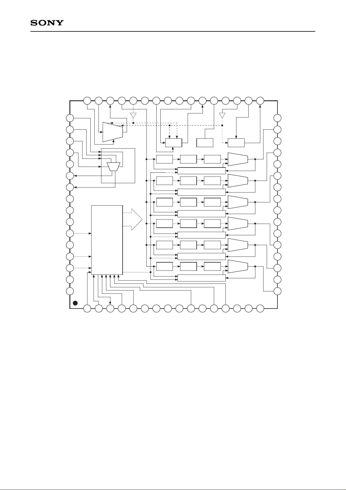
Block Diagram
POS_CNT1
POS_CNT2
NEXT_OUT
NEXT_IN
F/R_CNT
GND
NC
D.P
D.P
S/12_CNT
NC
ENB
DIR_CNT
NC
NC
NC
OFFSET
VIDEO_IN
INV_OUT
SH_IN
FRP
V
CC
SID_OFST
D.P
D.P
SID_IN
SID_OUT
ISET
NC
SIGCEN
VCOMOFST
VCOMOUT
GND2
SH_OUT1
NC
SH_OUT2
NC
SH_OUT3
PV
CC
D.P
D.P
PGND
NC
SH_OUT4
NC
SH_OUT5
NC
SH_OUT6
INV_CNT
DLY_CNT
MCLK
MCLK/
V
DD
CLK_OUT
CLK_OUT/
D.P
D.P
DGND
CLK_IN
NC
CLK_IN/
PRG
NC
NC
offset cancel
mode timing
S/H S/H S/H
OFFSET CANCEL
BUFFER
S/H S/H S/H
OFFSET CANCEL
BUFFER
S/H S/H S/H
OFFSET CANCEL
BUFFER
S/H S/H S/H
OFFSET CANCEL
BUFFER
S/H S/H S/H
OFFSET CANCEL
BUFFER
S/H S/H S/H
OFFSET CANCEL
BUFFER
SID BIAS VCOM
INVERT
AMP
CLOCK
DELAY
S/H
Pulses
TIMING
GENERATOR
31
32
17
18
19
20
21
22
23
24
25
26
27
28
29
30
2
3
4
5
6
7
8
9
10
11
12
13
14
15
16
1
40
39
38
37
36
35
34
33
41
42
43
44
45
46
47
48
49
50
51
52
53
54
55
56
57
58
59
60
63
64
61
62
D
– 3 –
CXA2112R
Pin Description
Pin
No.
Symbol I/O
Standard
voltage level
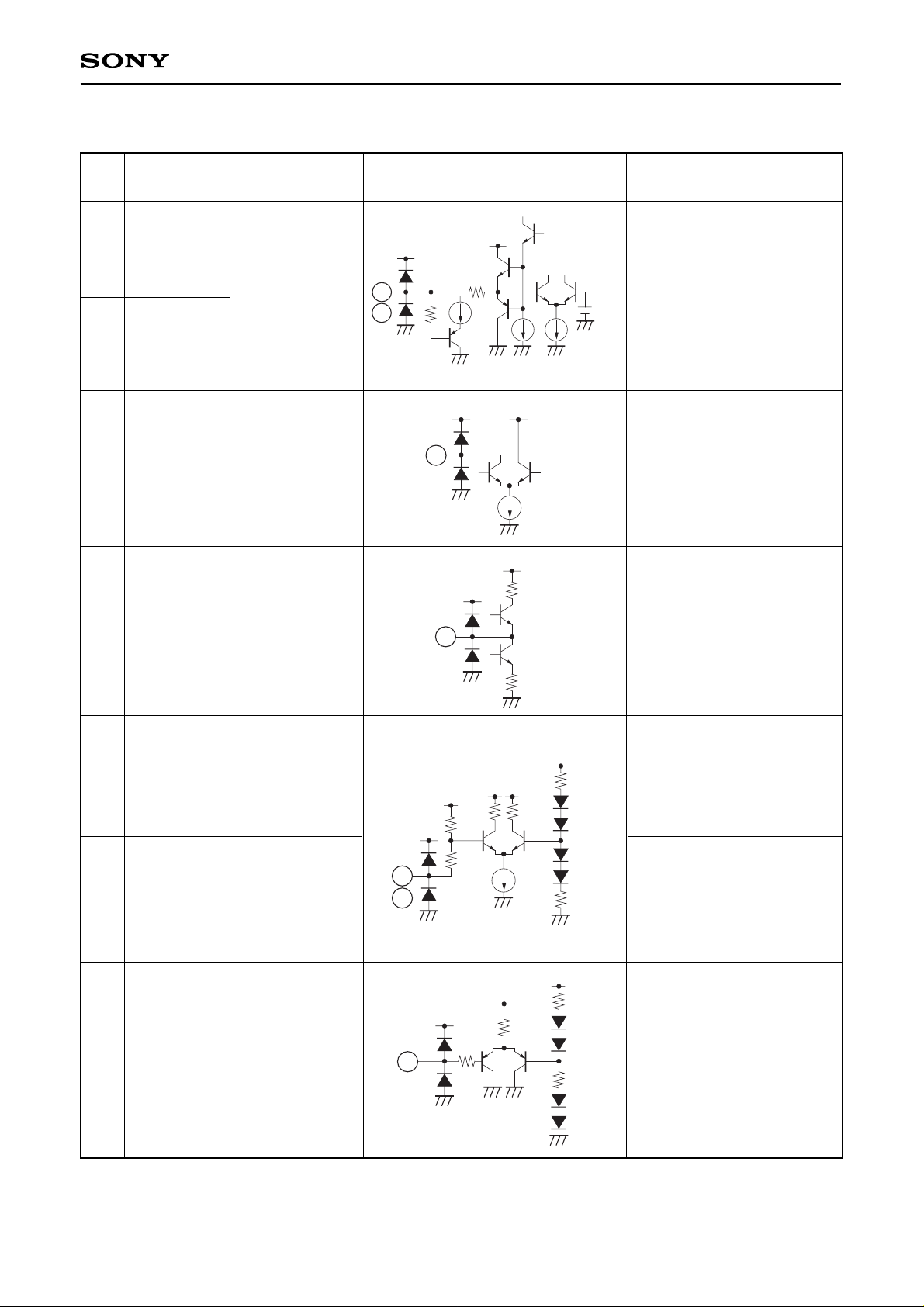
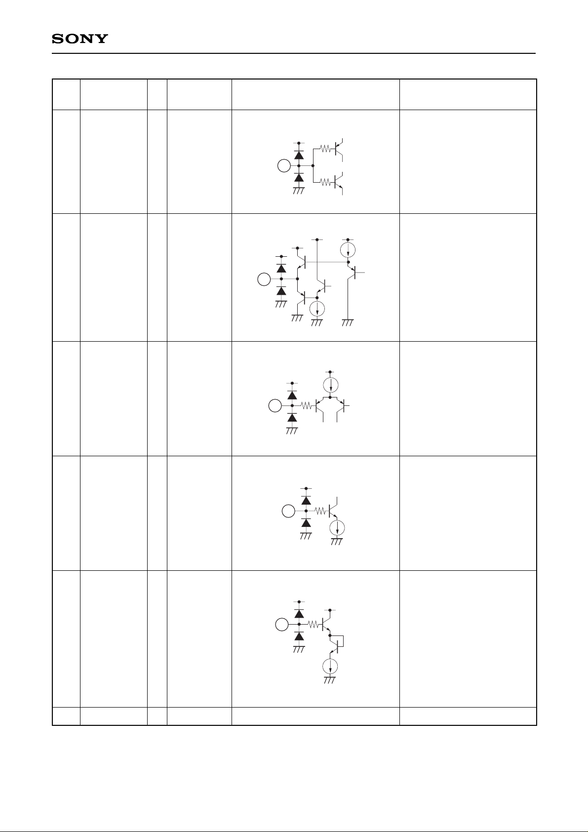
Equivalent circuit Description
1 POS_CNT1
2 POS_CNT2
I
See
Table A-1.
Sample-and-hold position
setting.
See Tables A-1, A-2 and A-3.
3 NEXT_OUT
O
Approx. 4V
Connect as closely as
possible to NEXT_IN.
4
NEXT_IN
I
Connect as closely as
possible to NEXT_OUT.
5 F/R_CNT
I
High: ≥ 2.5V
Low: ≤ 0.8V
OPEN High
Before/after decision for
12-output.
See Table B.
10 S/12_CNT
I
High: ≥ 2.5V
Low: ≤ 0.8V
OPEN High
6-output/12-output switch.
High: 6-output
Low: 12-output.
See Table B.
2k
20µ
60k
V
DD
VDD
20µ 10µ
1.6V
2
1
VDD
600µ
VDD
3
VDD
VDD
0.7k
16k
4
VDD
10k
VDDVDD
100k
VDD
VDD
100k
5
10
100k
20k
10k
25µ
12
ENB
I
High: ≥ 2.5V
Low: ≤ 0.8V
Horizontal sync signal ENB
input.
Refer to Timing Chart.
12
VDD
50k
V
DD
VDD
50k
150k
145
– 4 –
CXA2112R
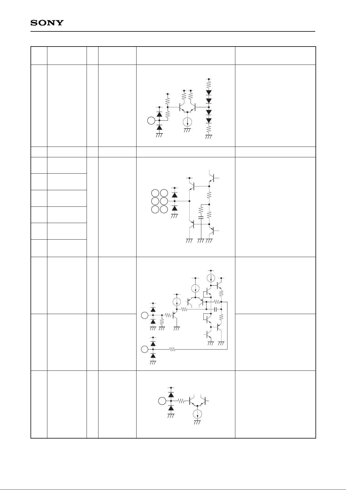
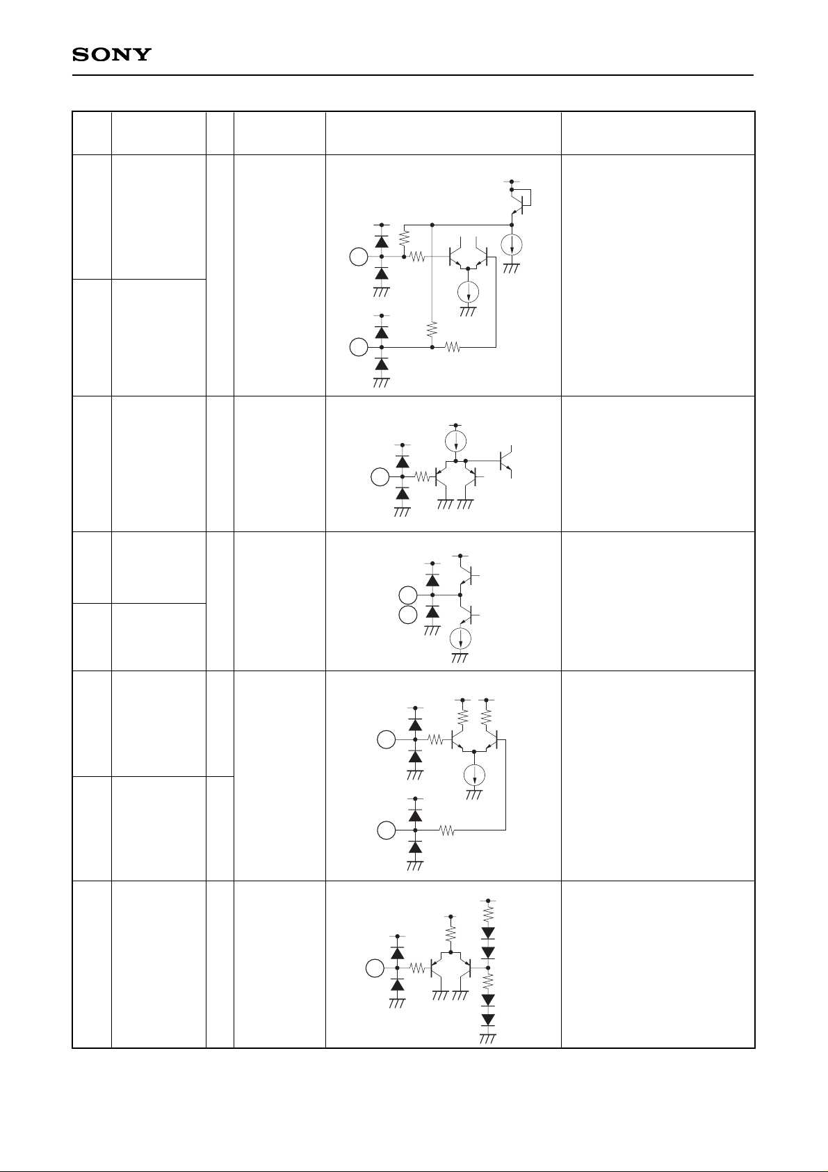
13 DIR_CNT
I
High: ≥ 2.5V
Low: ≤ 0.8V
OPEN High
Scan direction switch.
High: forward scan
Low: reverse scan
6 GND
17 SH_OUT6
19 SH_OUT5
21 SH_OUT4
27 SH_OUT3
29 SH_OUT2
3133SH_OUT1
VCOMOUT
O
O
GND
2.5 to 11.5V
5 to 8V
34 VCOMOFST
I
0 to 10V
Analog GND.
Output.
VCOM output.
Can be set to VSIGCEN to
VSIGCEN –2V by Pin 34 input.
VSIGCEN: voltage set by Pin 35.
VCOM output setting.
Deviation from SIGCEN
input is 0 for input setting of
0V. VCOM is set at the
minus side from VSIGCEN at
high voltage.
VDD
10k
VDDVDD
100k
VDD
VDD
100k
100k
20k
10k
25µ
13
21
PVCC
4k
4k
4k
2p
PV
CC
17
19
27
29
31
100k
10µ
2k
V
CC
VCC
VCC
VCC
VCC
500
1p
33
145
40k
VCC
70µ
80µ
500
200k
34
35 SIGCEN
I
7V
Center voltage of signal
inversion setting.
Output signal is inverted,
centered around this voltage,
by FRP high/low. Normally,
set to 7V.
VCC
20µ
35
10k
Pin
No.
Symbol I/O
Standard
voltage level
Equivalent circuit Description
– 5 –
CXA2112R
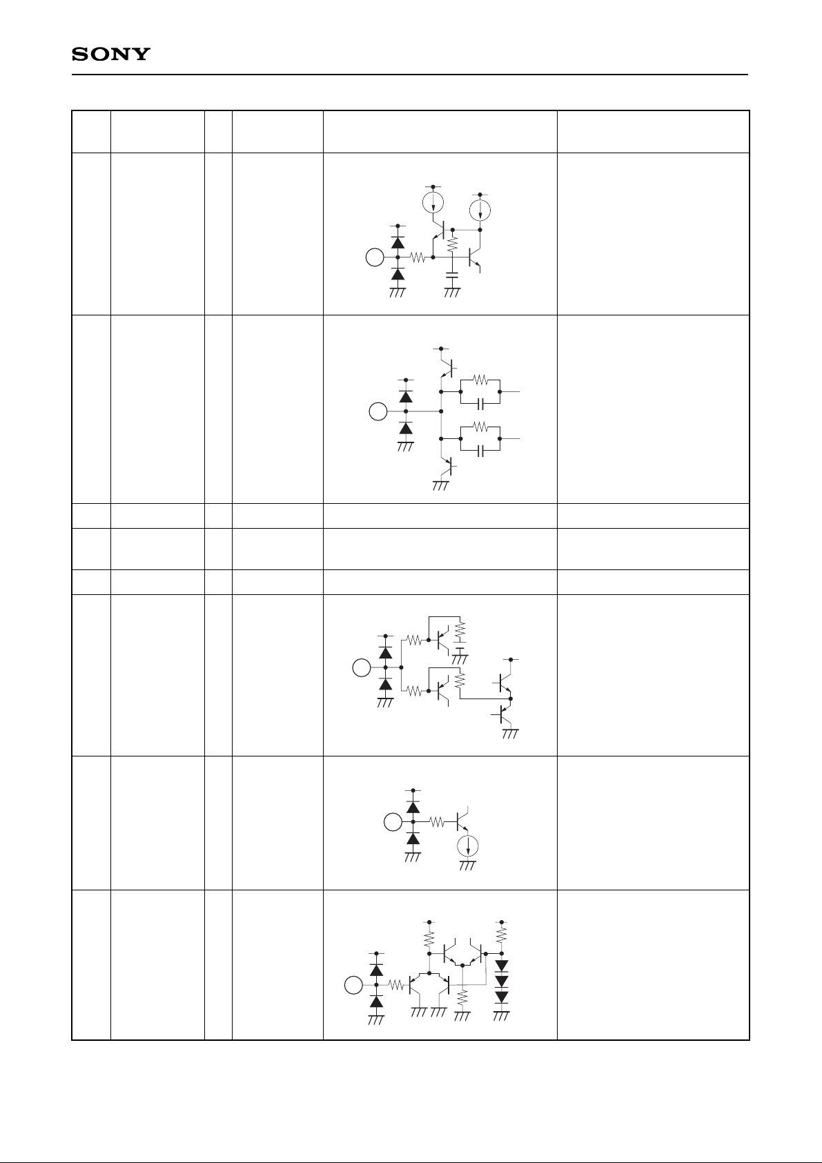
37
ISET
I
1.35V
Vcc circuit bias current
setting.
Normally, connect 27kΩ
(±1%) between this pin and
GND.
4p
145
V
CC
VCC
2k
37
VCC
10µ
45µ
38
SID_OUT
O
2.5 to 11.5V
SID signal waveform output.
Connect to an external
buffer for panel.
23 PGND
GND
26 PVCC
15.5V
32 GND2
GND
Power GND.
Power Vcc.
Connect directly to Vcc.
Analog GND.
39 SID_IN I 2.3 to 3.3V
SID signal input.
VCC
VCC
75k
0.2p
0.2p
75k
38
91k
V
CC
7V
39
19.5k
19.5k
78k
VCC
42 SID_OFST
I
3.3V
SID signal input offset
setting.
44
FRP
I
High: ≥ 2.5V
Low: ≤ 0.8V
Invert pulse input.
High: inverse
Low: non-inverse
Refer to Timing Chart.
VCC
10µ
30k
42
VDD
50k
V
DD VDD
100k
10k
50k
44
Pin
No.
Symbol I/O
Standard
voltage level
Equivalent circuit Description
– 6 –
CXA2112R
45 SH_IN
I
2.5 to 11.5V
Sample-and-hold circuit
common input.
Should not be less than 2V.
46 INV_OUT
O
2.5 to 11.5V
Invert amplifier output.
VCC
1.9k
200
45
46
VCC
VCC
620µ
VCC VCC
560µ
47 VIDEO_IN
I
2.0 to 3.3V Invert amplifier input.
48
OFFSET
I
3.3V
Video signal input offset
setting.
Inputs 100% white level.
49
DLY_CNT
I
3 to 5V
Dot clock phase adjustment.
43 VCC
15.5V
15V power supply.
145
300µ
V
CC
VCC
47
30k
10µ
VCC
48
2k
50µ
VDD
VDD
49
Pin
No.
Symbol I/O
Standard
voltage level
Equivalent circuit Description
– 7 –
CXA2112R
50 MCLK
51 MCLK/
I
PECL
differential
Dot clock input.
20k
1k
V
DD
VDD
10µ
VDD
50
51
20k
1k
100µ
52 INV_CNT
I
High: ≥ 2.5V
Low: ≤ 0.8V
Dot clock phase invert
control.
VDD
VDD
2k
52
10µ
54 CLK_OUT
55 CLK_OUT/
I
VDD – 0.3V
to VDD
Phase adjusted dot clock
output.
62
PRG
I
High: ≥ 2.5V
Low: ≤ 0.8V
Horizontal sync signal PRG
input.
Refer to Timing Chart.
59 CLK_IN
I
61
CLK_IN/
I
VDD – 0.3V
to VDD
On-chip timing generator
clock input.
Connect directly to Pins 54
and 55.
55
1m
V
DD
VDD
54
VDD
VDD
100µ
VDD VDD
59
61
2k
2k
145
145
VDD
VDD
145
VDD
150k
50k
50k
62
Pin
No.
Symbol I/O
Standard
voltage level
Equivalent circuit Description
 Loading...