

Sony CXA2108AQ Datasheet

CXA2108AQ
Constant-Current Driver for Full Color LED Display
Description
The CXA2108AQ is a 1,024-gradation LED driver
which is ideal for full color LED displays. This IC has
24 outputs and a maximum output current of 70mA.
Time division allows driving of either two or six LEDs
per output by connecting an external FET or other
switch. The luminance (PWM) and drive current for
each LED are set using the internal RAM. The LED
type is common anode.
Features
• 24 outputs: 10-bit (1,024-gradation) PWM current outputs
• Maximum output current: 70mA
• LED type: Common anode
• 4-bit brightness function capable of switching the basic PWM pulse width in 16 steps
• Time division allows driving of up to six LEDs with a single output, making it possible to configure a high
definition display with few driver ICs.
• Coarse Adj. (2 bits) and Fine Adj. (8 bits) output current adjustment for each LED makes it possible to drive
R, G and B using the same output from the same IC. In addition, the characteristics variance of each LED
can also be corrected.
• All luminance (PWM) data and drive current data are set by writing to the internal RAM.
• PWM emitting can be performed up to 15 times per frame to realize a screen with little flicker.
• Two built-in PWM data RAM make it possible to set the next luminance data even during PWM operation.
• Abnormal internal temperature detection circuit
• Single 5V power supply
• Current output with protection diode (diode cathode voltage: VPD can be supplied independently of the 5V
power supply.)
• Surface mounting package (80-pin QFP)
Applications
LED display panels
Structure
Bi-CMOS silicon monolithic IC
Absolute Maximum Ratings (Ta = 25°C)
• Supply voltage AVCC, DVCC –0.3 to +6.0 V
VPD –0.3 to +10.5 V
• Digital input voltage VI_D –0.3 to DVCC + 0.3 V
• Digital output current Io_D –5.0 to +5.0 mA
• Driver output voltage V_DVR 0 to VPD + 0.3 V
• Driver output current I_DVR –1 to +80 mA
• Operating temperature
∗1
Topr –40 to +80 °C
• Storage temperature Tstg –65 to +150 °C
• Allowable power dissipation∗1(Ta = 65°C or less) PD 1.5 W
Recommended Operating Range
• Supply voltage AVCC, DVCC 4.75 to 5.25 V
VPD AVCC to 10 V
• Driver output compliance voltage Vcmp 1.0 to VPD + 0.3 V
(I_DVR = 0 to 70mA)
• Operating temperature (ambient temperature)
∗1
Ta –20 to +65 °C
• Operating temperature (case temperature)
∗1
Tc –20 to +110 °C
∗1
When mounted on a printed circuit board
– 1 –
E99160-PS
Sony reserves the right to change products and specifications without prior notice. This information does not convey any license by
any implication or otherwise under any patents or other right. Application circuits shown, if any, are typical examples illustrating the
operation of the devices. Sony cannot assume responsibility for any problems arising out of the use of these circuits.
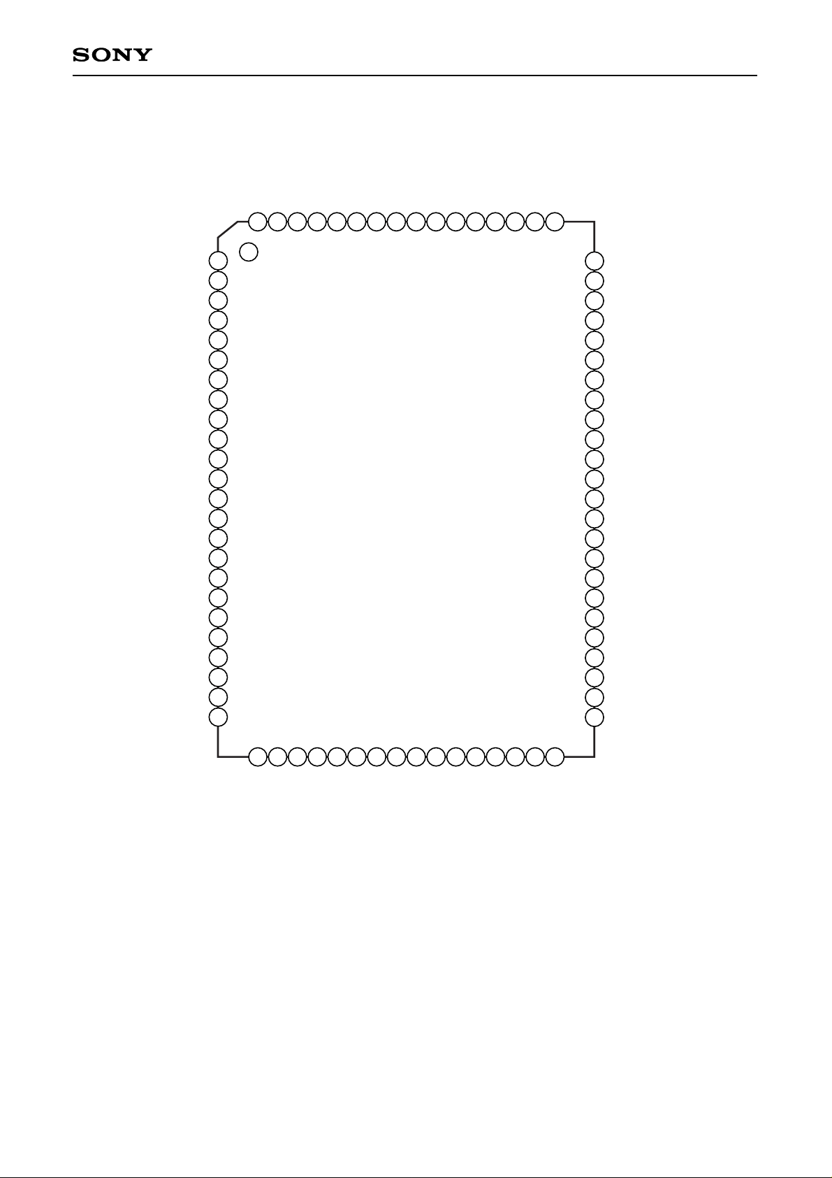
80 pin QFP (Plastic)
– 2 –
CXA2108AQ
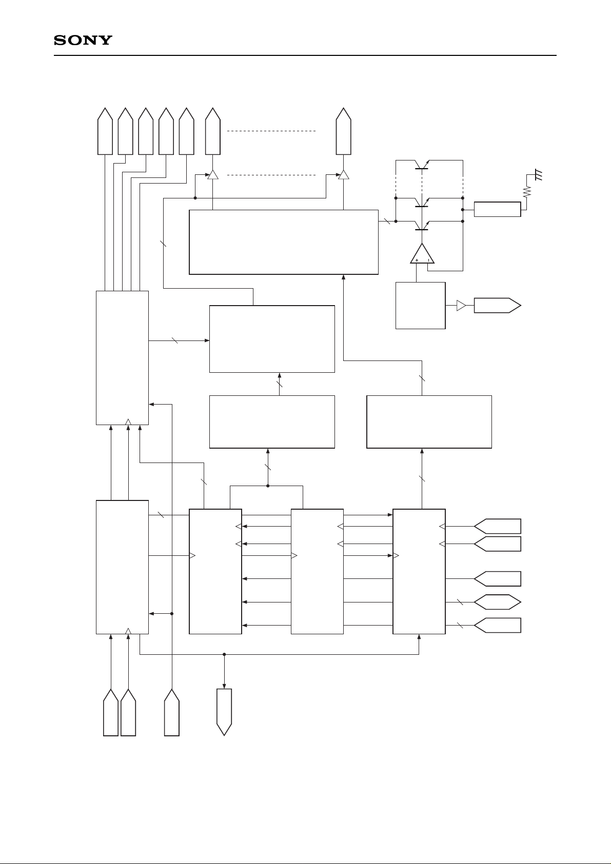
Block Diagram
PWM data RAM (B)
(6word × 24ch × 10bit)
PWM data RAM (A)
(6word × 24ch × 10bit)
Data Read Counter
Drive Current data RAM
(6word × 24ch × 10bit)
10bit × 24
Shift Reg.
&
Latch
PWM data
10bit × 24
Shift Reg.
&
Latch
8bit DAC with
2bit coarse Adj.
(× 24)
× 24
DLDI
CLK
IOUT23
A0 to 9
10
MODE
RDY
D0 to 9
XTAO
REXT
XR/W
XRD
XWR
10
10
DATA
10 × 24
Rext
24
10 × 24
24
PWMout
PWM Counter
10
DATA
4
10
Counter
out
Data
Comparator
Band
Gap
Ref.
9
BRT
R_ADRR_CLK
IOUT0
XB
XG
XR
XUPR
DLDO
Drive
Current
data
– 3 –
CXA2108AQ
Pin Configuration (Top View)
25 26 27 28 29 30 31 32 33 34 35 36 37 38 39
40
45
46
47
48
49
50
51
52
53
54
55
56
57
58
59
60
61
62
63
64
65666768697071727374757677787980
1
2
3
4
5
6
7
8
9
10
11
12
13
14
15
16
17
18
19
20
D1
D2
D3
D4
D5
D6
D7
D8
D9
A0
A1
A2
A3
A4
A5
A6
IOUT5
IOUT4
IOUT3
IOUT2
IGND
IOUT1
IOUT0
AV
CC
AGND
REXT
NC
NC
XTAO
XRST
XR/W
XRD
XWR
XCS
DLDI
A9
41
42
43
44
A8
DV
CC
DGND
A7
IOUT18
IOUT19
IOUT20
IOUT21
IGND
IOUT22
IOUT23
AV
CC
AGND
VPD
MODE
DGND
RDY
DLDO
21
22
23
24
CLK
DGND
DV
CC
D0
WALL
XUPR
TEST_O
XB
XR
XG
IOUT17
IGND
IOUT16
IOUT15
IOUT14
IGND
IOUT13
IOUT12
IOUT11
IOUT10
IGND
IOUT9
IOUT8
IOUT7
IGND
IOUT6
– 4 –
CXA2108AQ
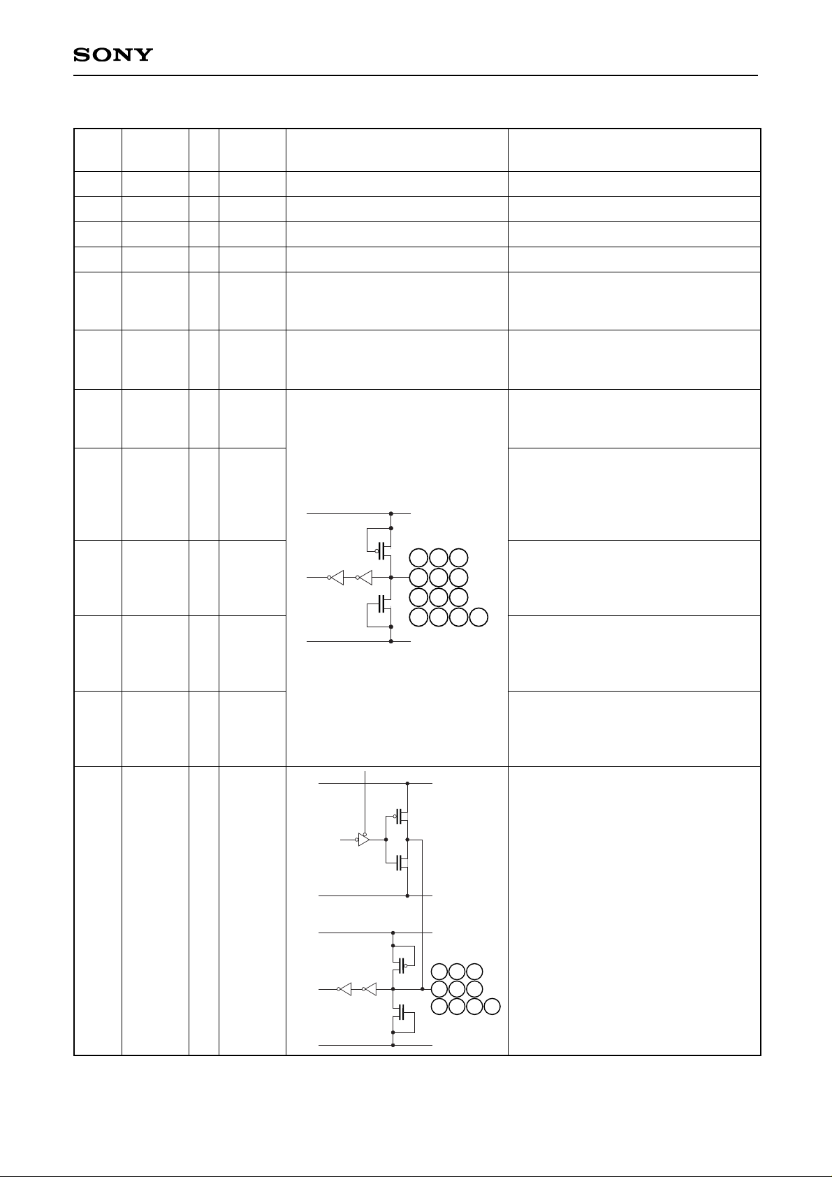
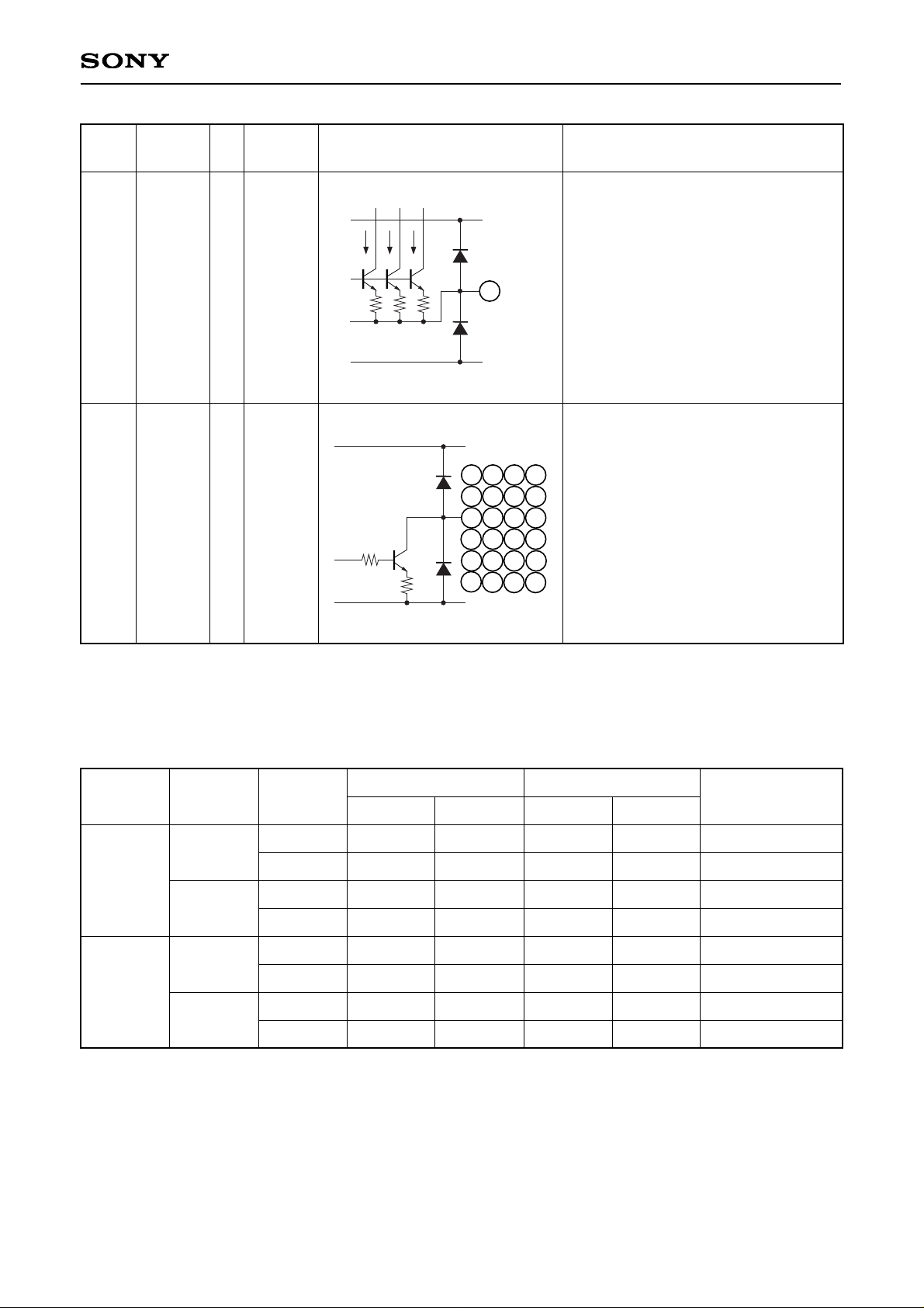
Pin
No.
Symbol Equivalent circuit Description
Reference
voltage
level
I/O
Pin Description
Analog GND.
9, 56
AGND
GND
—
Analog power supply.
8, 57
AVCC
5V (Typ.)
—
Digital GND.
12, 22, 42
DGND
GND
—
Digital power supply.
23, 43
DVCC
5V (Typ.)
—
GND for driver output.
5, 60,
66, 70,
75, 79
IGND
GND
—
Open.
This pin is not connected with the
internal circuits.
53, 54
NC
DGND
DV
CC
40
37
34
21
41
38
35
51
44
39
36
11
45
—
Clock input.
Driver operation is synchronized with
this clock.
Reset input.
The IC is initialized by inputting low
level. However, the memory is not
initialized. Input high level during
normal operation.
Output mode switching.
Upper/Lower mode for low level input.
Upper/Lower/RGB mode for high level
input. (See the Description of Operation.)
Address input.
These pins are used to input the internal
RAM (luminance data, brightness data
and drive current data RAM) address.
RAM selection.
The luminance data RAM is selected
when this pin is low, and the drive
current data RAM when high.
21
CLK
CMOS
I
51
XRST
CMOSI
11
MODE
CMOS
I
34 to 41,
44
A0 to 8
CMOS
I
45
A9
CMOSI
DGND
DV
CC
30
27
24
31
28
25
32
29
26
33
DGND
DV
CC
Data I/O.
These pins are used to input and
output data to and from the internal
RAM (luminance data, brightness data
and drive current data RAM). See
Table 1. Read/Write Switching
Condition Correspondence Table for
the data I/O switching conditions.
24 to 33
D0 to 9
CMOS
I/O

– 5 –
CXA2108AQ
Internal RAM chip select.
Internal RAM access is enabled by
inputting low level. (See Table 1.
Read/Write Switching Condition
Correspondence Table.)
Internal RAM read/write select.
Write mode is selected for high level, and
read mode for low level. See Table 1.
Read/Write Switching Condition
Correspondence Table for the actual
read/write switching signal input conditions.
Write clock input.
This pin is used to input the clock for
writing the luminance, brightness and
drive current data. It is not
synchronized with CLK.
Read clock input.
This pin is used to input the clock for
externally reading the luminance,
brightness and drive current data. It is
not synchronized with CLK.
Trigger signal input for luminance data
RAM (A)/(B) switching and PWM
output start.
(See the Timing Charts.)
47
XCS
CMOS
I
50
XR/W
CMOS
I
48
XWR
CMOS
I
49
XRD
CMOS
I
46
DLDI
CMOS
I
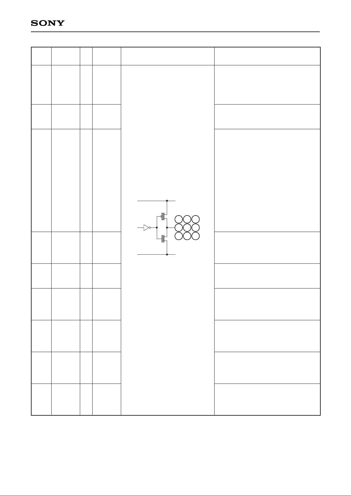
Pin
No.
Symbol Equivalent circuit Description
Reference
voltage
level
I/O
Voltage supply terminal for cathode of
positive protection diode which
connected to drivers (IOUTO to
IOUT23) and REXT (55pin).
Normally,connect to LED DC supply.
However ,when the LED DC supply
voltage exceeds 10V,VPD must be set
10V or less.
10 VPD
5V (Typ.)
—
CC
DV
47 48
494650
DGND
– 6 –
CXA2108AQ
READY signal output.
This indicates the drive current data
RAM access enabled period. Access
is enabled while high level is output.
(See the Timing Charts.)
DLDI signal output.
This outputs the DLDI signal
synchronized with CLK.
Write ALL signal output.
One pulse (= high level signal with a
width of 1 clock) is output
synchronized with the rising edge of
the next CLK after the final address
∗1
of the currently selected mode is input.
Note that both the final address must
be input and the XCS and XWR input
levels must be low at the rising edge
of this CLK.
(See the Timing Charts for details.)
∗1
02Fh (Upper/Lower mode)
08Fh (Upper/Lower/RGB mode)
Upper signal output.
This is used as the LED switching signal.
(See the Timing Charts and Application
Circuits for details.)
Test signal output.
This pin is unrelated to the functions of this IC.
Do not connect anything; leave this pin open.
Blue signal output.
This is used as the LED switching signal.
(See the Timing Charts and Application
Circuits for details.)
Red signal output.
This is used as the LED switching signal.
(See the Timing Charts and Application
Circuits for details.)
Green signal output.
This is used as the LED switching signal.
(See the Timing Charts and Application
Circuits for details.)
Thermal Alarm Out signal output.
This pin normally outputs high level, but it
outputs low level when the internal
temperature rises to an abnormally high level.
13
RDY
CMOS
O
14 DLDO CMOSO
15
WALL
CMOS
O
16
XUPR CMOS
O
17 TEST_O
CMOS
O
18
XB CMOSO
19
XR
CMOS
O
20 XG
CMOS
O
52 XTAO
CMOS
O
Pin
No.
Symbol Equivalent circuit Description
Reference
voltage
level
I/O
13
16
19
DV
14
17
20
CC
15
18
52
DGND
– 7 –
CXA2108AQ
Drivers.
These pins drive the LED.
1 to 4,
6, 7,
58, 59,
61 to 65,
67 to 69,
71 to 74,
76 to 78,
80
IOUT0
to 23
O
XCS
[ I ]
L
H
XR/W
[ I ]
L
H
L
H
A9
[ I ]
L
H
L
H
L
H
L
H
Luminance
Write
Disable
Disable
Enable
Disable
Disable
Disable
Disable
Disable
Enable
Disable
Disable
Disable
Disable
Disable
Disable
Disable
Disable
Disable
Disable
Enable
Disable
Disable
Disable
Disable
Disable
Enable
Disable
Disable
Disable
Disable
Disable
Disable
Read
Drive current
D0 to 9
[I/O]
Output
Output
Input
Input
Hi-Z
Hi-Z
Hi-Z
Hi-Z
Write Read
Table 1. Read/Write Switching Condition Correspondence Table
AGND
VPD
55
Drive current setting.
Connect a resistor between this pin
and GND. The drive current is
proportional to the current flowing to
this resistor. (See Table 2. Drive
Current Setting and Power
Consumption.)
55
REXT
O
Pin
No.
Symbol Equivalent circuit Description
Reference
voltage
level
I/O
VPD
1 2 3 4
6 7 58 59
61 62 63 64
67 68 69
65
71 72 73 74
76
77
IGND
78 80
– 8 –
CXA2108AQ
Rext [kΩ] D9 D8 Io (FFh) [mA] Istb [mA] Pstb [W] Po (max) [W]
∗1
Absolute maximum rating exceeded.
Table 2. Drive Current Setting and Power Consumption (when D0 to D7 = FFh)
Rext : External resistor that sets the DAC reference current (Iref)
D9, D8 : Data that sets the maximum drive current (Io (FFh))
Iref : DAC reference current
Iref [mA] = 1.3 [V]/Rext [kΩ]/24
Io (FFh) : Maximum drive current that can be set by D0 to D7
Io (FFh) [mA] = Iref × (2 × D9 + D8 + 1) × 800
Istb : Standby current (Internal current consumption excluding the driver block)
Istb [mA] = 3.06 + 24 × Iref × (16/3 + 24.25 × (2 × D9 + D8 + 1))
Pstb : Standby power (Internal power consumption excluding the driver block, Vcc = 5 V)
Pstb [W] = 5 [V] × Istb [mA]/1000
Po (max)
: Maximum power that can be consumed by the driver block
Po (max) [W] = 1.5 [W] – Pstb [W]
Note) Istb, Pstb and Po (max) are the values when D0 to D7 = 11111111 (FFh).
In addition, these values assume the case where all channels are set to the same drive current.
2.0
2.0
2.0
2.0
2.5
2.5
2.5
2.5
3.0
3.0
3.0
3.0
3.5
3.5
3.5
3.5
4.0
4.0
4.0
4.0
0
0
1
1
0
0
1
1
0
0
1
1
0
0
1
1
0
0
1
1
0
1
0
1
0
1
0
1
0
1
0
1
0
1
0
1
0
1
0
1
21.7
43.3
65.0
86.7
∗1
17.3
34.7
52.0
69.3
14.4
28.9
43.3
57.8
12.4
24.8
37.1
49.5
10.8
21.7
32.5
43.3
22.3
38.1
53.8
69.6
18.4
31.1
43.7
56.3
15.9
26.4
36.9
47.4
14.0
23.1
32.1
41.1
12.7
20.6
28.4
36.3
0.111
0.190
0.269
0.348
0.092
0.155
0.218
0.281
0.079
0.132
0.184
0.237
0.070
0.115
0.160
0.205
0.063
0.103
0.142
0.182
1.39
1.31
1.23
1.15
1.41
1.34
1.28
1.22
1.42
1.37
1.32
1.26
1.43
1.38
1.34
1.29
1.44
1.40
1.36
1.32
– 9 –
CXA2108AQ
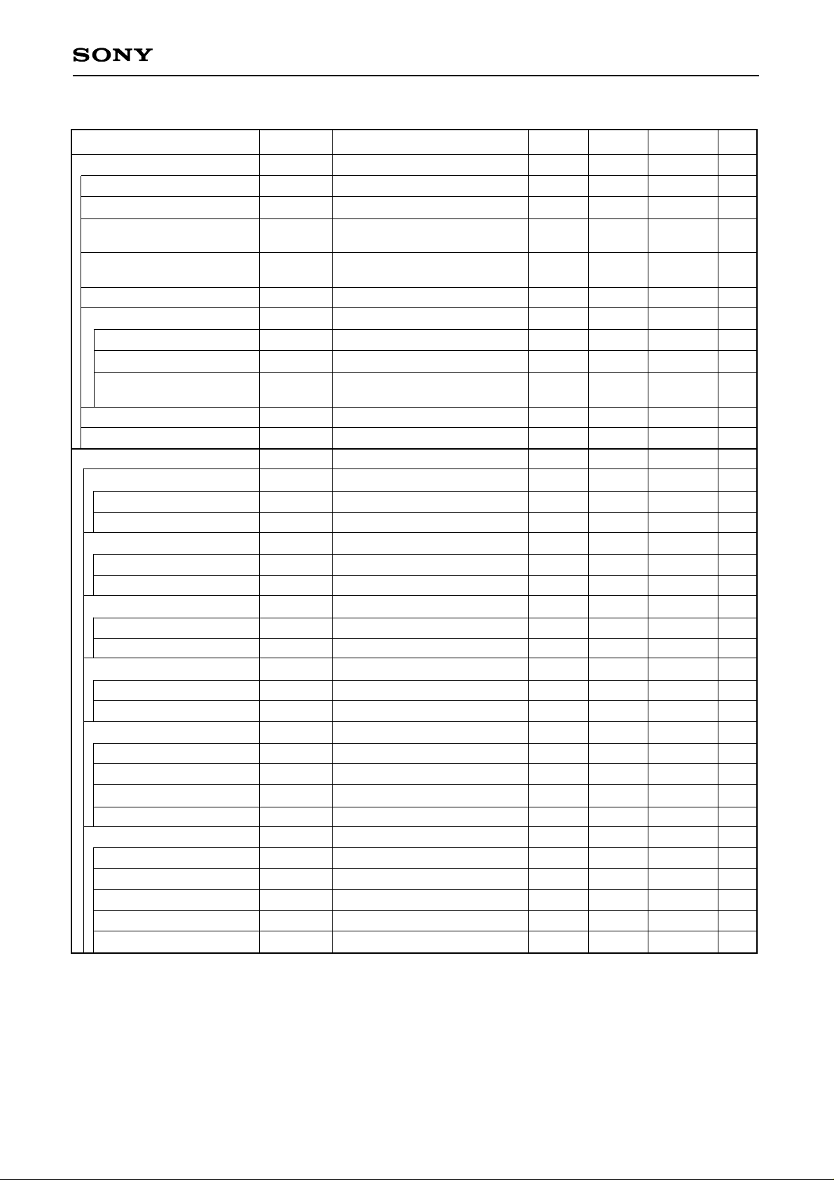
Electrical Characteristics (AVCC, DVCC = +5V, VPD = +10V, AGND, DGND, IGND = 0V)
PWM output resolution
bit
10
Drive current setting resolution
Coarse Adj.
bit
2
Fine Adj.
bit
8
DLE ±0.8
Io (FFh) = 60mA
(D0 [LSB] to D7 [MSB] = FFh)
DC characteristics
Differential linearity error
LSB
fCLK
15
PWM reference clock frequency
MHz
Item
Symbol
Conditions
Min.
Typ.
Max.
Unit
Driver block
VREXT
1365
1235
Rext = 2kΩ
REXT pin voltage
mV
1300
∆VREXT
20
0
VREXT (@AVCC = 5.25V)
– VREXT (@AVCC = 4.75V)
REXT pin voltage
Supply voltage dependency
mV
ICC
30
20
Rext = 2kΩ, D8 = D9 = 0
Note) Excluding the driver block
Standby supply current
mA
IOUT
70
Output current
mA
Output compliance voltage
Logic block
Digital input current (I, I/O)
Vcmp
VPD + 0.3
1
Io = 0 to 70mA
V
(H)
IIH
5
–5VIN = 5V
µA
(L)
IIL
5
–5
VIN = 0V
µA
Digital input voltage (I, I/O)
(H)
VIH
DVCC + 0.3
0.7DVCC
V
(L)
VIL
0.3DVCC
–0.3
V
Digital output voltage (O)
(H)
VOH
4DVCC = 5V, IOH = –2mA V
(L)
VOL
0.4
DVCC = 5V, IOL = 4mA
V
Digital output voltage (I/O)
(H)
VOZH
3.7
DVCC = 5V, IOH = –2mA
V
(L)
VOZL
0.4
DVCC = 5V, IOL = 4mA
V
RAM write mode
Write cycle
TWR
133.3
ns
Write pulse width
TCWR
55
ns
Setup time TSWR 10 ns
Hold time THWR 10
ns
RAM read mode
Read cycle
TRD
133.3
ns
Read pulse width
TCRD
55
ns
Setup time
TSRD
10
ns
Hold time
THRD
10
ns
Output delay time
TPDD
100Output load 50pF or less ns
 Loading...